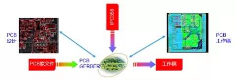
As an important link in hardware design, PCB Layout is an absolutely important index affecting performance when the hardware circuit design is reasonable. Many PCB Layout engineers complete the Layout and wiring according to the constraint rules given by hardware engineers or PI SI engineers. These are commonly known as “wire pullers”. After a period of time, some of them may have some experience: which ones should be equal length, which ones should be thick, which ones should be parallel, ensure proper line spacing and so on. However, they rely on so-called experience, and many of them do not know why. I love solutions. If you want to make a breakthrough, you have to broaden your knowledge. PCB Layout engineer should not let others regard him as a “wire worker”.
Some principles from some PCB designs(PCB Layout knowledge):
- Layout is to place circuit components reasonably. Then how to place is reasonable, a simple principle is clear modular division, that is to say, people with a certain circuit foundation, get your PCB can see which piece is used to achieve what function.
- Specific design steps: first, generate initial PCB file according to schematic diagram, complete PCB pre-layout, determine a relative PCB Layout area, and then tell the structure, the structure according to the area we give, and then give specific constraints according to the overall structure design.
- According to the constraints of the structure, complete the drawing of plate edges, positioning ports and some forbidden areas, and then complete the placement of connectors.
- Component placement principle: In general, the main control MCU is placed in the center of the board, and then the interface circuit is placed close to the interface (such as network port, USB, VGA, etc.), and most of the interfaces have ESD protection and filtering processing. The principle followed is protection before filtering.
- Then there is the power module. Generally, the main power module is placed at the power supply entrance (such as system 5V), and the discrete power module (such as 2.5V power supply of the module circuit) can be placed in the place where the same power network is more dense according to the actual situation.
- Some internal circuits are not connected to connectors. We generally follow such a basic principle: high-speed and low-speed areas, analog and digital areas, interference sources, sensitive receptor areas.
- Then for individual circuit modules, follow the current direction of the circuit design.
The basic requirement for wiring is to ensure that all networks are connected effectively. Connectivity is easy to do, and efficiency is a nebulous concept. In fact, there are no more than two kinds of signals in the circuit: digital signal and analog signal, for digital circuit is to ensure enough noise tolerance, for analog signal, as far as possible to achieve zero loss.
Before wiring, it is generally necessary to understand the cascade design of the whole PCB board, that is, all wiring layers are planned as: optimal wiring layer, sub-optimal wiring layer… , the optimal wiring layer, that is, the adjacent interview complete ground plane, this layer we generally used to distribute important signals (including all signals in DDR, differential signals, analog signals and so on). Other signals (I2C, UART, SPI, GPIO) go through other layers, and ensure that only signals related to this circuit (such as DDR and network port) exist in important areas. Then high-speed signal wiring needs to consider reflection, crosstalk, EMC and other problems, so generally need to do impedance matching, such as single line 50R, difference line 100R and so on, the specific design shall be subject to (the principle is to ensure equal and continuous impedance), crosstalk mainly consider 3W/2W principle, ground enveloping processing and so on.
Power supply and power circuit, first of all, to ensure enough carrying capacity, that is, the power supply of the entire backflow circuit strength as thick and short as possible, from the EMC perspective, backflow loop, loop antenna, external radiation, so as to reduce the loop area.
Grounding and ground design are very important in PCB design, because ground is an important reference plane, if there is a problem with the ground plane design, other signals can not be stable.
The ground is generally divided into chassis and system. Chassis, as the name implies, is the ground to which the sheet metal of the product is connected, and systematically is the reference plane of the whole circuit system.
The practical principle of the general system and the housing is: the housing and the system are separated, and then the system is connected through the magnetic beads and the high voltage capacitor single point or multi-point.
On the system: it can be divided into digital, analog and power functions.
First of all, the layout is very reasonable, I think the ground can not be divided. What is the layout is very reasonable, that is, there are only digital signals in the digital area, only analog signals in the analog area, only power signals in the power area, and there are complete ground planes below them. Because electricity and water flow are very similar, they both flow downward, and there is a whole plane of the earth beneath them, so from the shortest to the lowest principle, they flow directly under the bottom, and do not go to other places.
However, sometimes, it is not so ideal, and there is some crossover in each area. In this case, single point understanding is generally selected and 0R resistance is used (magnetic beads are not recommended, because they have filtering effect at high frequency). The position of resistors is close to the place where the cross is most dense, and the flow area is the smallest.