SMT stencil ( PCB Files & BOM List, please send to [email protected] ( Fast Quote ) . For more information kindly check our website: www.winowpcba.com
A surface mount technology (SMT) stencil may also be called a PCB sentil, solder paste stencil, or laser stencil.
A SMT Stencil’s main purpose is to simply transfer the solder paste to a bare circuit board.
A stainless steel foil is laser cut to create an opening for each surface mount device on the board.
Once the printed circuit board (PCB) stencil is properly aligned with the top of the board, the solder paste is applied over the openings (in a single pass, with a metal squeegee).
When the stainless steel foil detaches from the board, solder paste remains, ready for the manufacture of the surface-mount device (SMD). In contrast to manual soldering procedures, this process ensures consistency and saves time.
Laser stencil PCB
The deposited solder paste released to the board is manipulated by opening the size of the aperture, and the thickness of the SMT stencil is made out of stainless steel.
Excessive paste will cause problems for connectivity and bridging, whereas less paste will compromise the strength of the soldering and joints.
The thickness of an SMT stencil varies with the device for which it is being used. 0.020” pitch small outline integrated circuits (SOICs) can work better with a stencil giving a thin solder paste, whereas thick solder paste works best with 0.050” pitch SOICs.
The thickness of the paste stencil for solder ranges from 0.001” to 0.003”. The normal thickness for most of the PCB boards is generally between 0.004” and 0.007”.
Stencil design of surrounding pads
The thickness of the stencil determines the amount of solder paste printed on the PCB. Too much solder paste will cause bridging during reflow soldering.
Therefore, it is recommended that the 0.5mm pitch QFN package use a 0.12mm thick steel mesh, and the 0.65mm pitch QFN package use a 0.15mm thick steel mesh.
The size of the stencil opening can be appropriately smaller than that of the pad to reduce the occurrence of solder bridging.
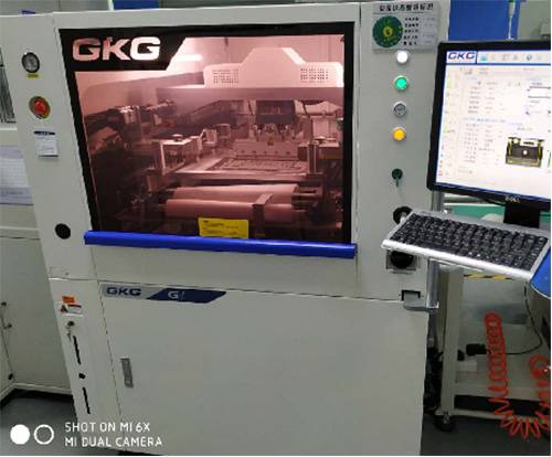
Circuit Board Stencil
Whether to get perfect and reliable solder joints, printing your stencil design is the key first step. The opening size of the surrounding pad stencil is directly related to the thickness of the stencil. Generally, thicker stencils can be designed with an opening slightly smaller than the pad size, while the opening size of the thinner stencil can be designed1:1. It is recommended to use a laser to make a steel mesh with openings and electropolishing.
