| Capabilities | Standard Production |
|---|---|
| Build-up Layers | 3+N+3 |
| Buried Core (reinforced) | 2 Layer/Multilayer, 100um thick minimum |
| Build-up Film Dielectric Thickness | 25um ~ 40um |
| Build-up Material | AFT GX-series |
| Core Via Interconnect | Laser Through Via, Mechanical Through Via |
| Build-up Laser Via Interconnect | Laser Blind Via, 60um diameter |
| Core Layer Copper Thickness | 25um typical |
| Core Layer Line/Space (subtractive) | 40um/60um minimum |
| Build-up Layer Copper Thickness | 18um nominal (typical) |
| Build-up Layer Line/Space (SAP) | 9um/12um minimum |
| Solder Resist | Roller Coated Liquid, Laminated Film |
| Surface Finish | ENEPIG |
| C4/micro-bump pitch (Pb free solder) | 90um minimum |
| Land Site Devices (chip passives) | 01005 minimum body size |
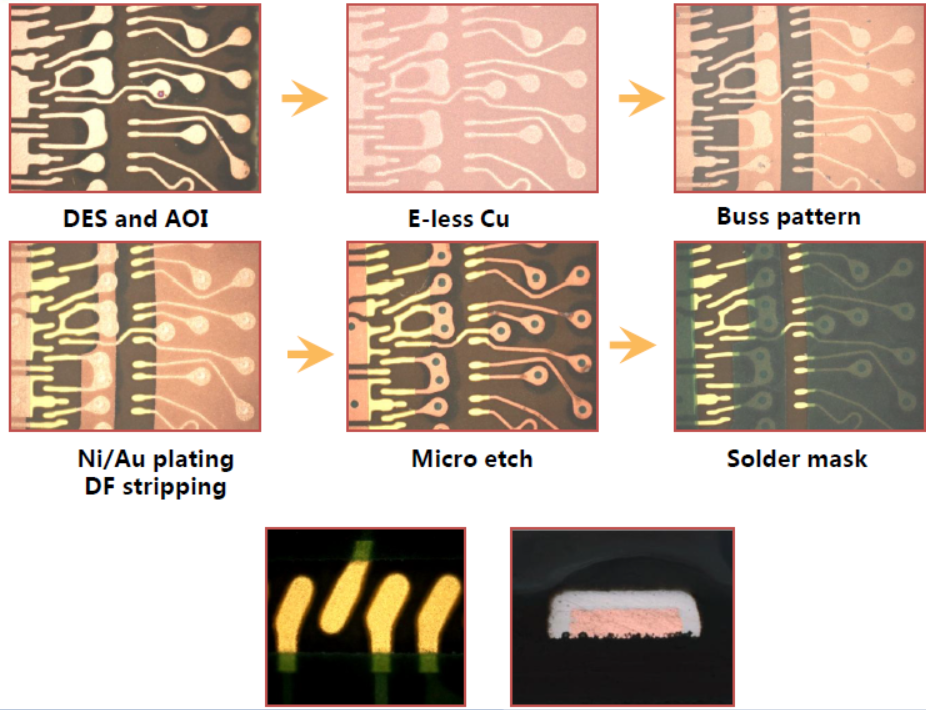
Capabilities Of ICS
IC substrate PCB has been developing with the booming of new types of ICs like BGA (ball grid array) and CSP (chip scale package) which call for new carriers of package. As one type of the most advanced PCB (Printed Circuit Board), IC substrate PCB has exploded in both popularity and applications together with any layer HDI PCB and flex-rigid PCB, now widely applied in telecommunications and electronics updates.