PCB production process, that is, printed circuit board production process. Almost every electronic device, ranging from electronic watches and calculators to large computers, communication electronic equipment, and military weapon systems, as long as there are electronic components such as integrated circuits, printed boards are used for the electrical interconnection between them. In a larger electronic product research process, the most fundamental success factor is the design, documentation, and manufacture of the product’s printed board. The design and manufacturing quality of printed boards directly affect the quality and cost of the entire product, and even lead to the success or failure of business competition.
Printed circuits provide the following functions in electronic equipment
Provide mechanical support for fixing and assembling various electronic components such as integrated circuits.
Realize wiring and electrical connection or electrical insulation between various electronic components such as integrated circuits.
Provide the required electrical characteristics, such as characteristic impedance, etc.
Provide solder mask graphics for automatic soldering, and provide identification characters and graphics for component insertion, inspection, and maintenance.
Some basic terms related to printed boards are as follows
On the insulating substrate, according to a predetermined design, a printed circuit, a printed component or a conductive pattern formed by combining the two is made, which is called a printed circuit.
On the insulating substrate, the conductive patterns that provide electrical connections between components and devices are called printed circuits. It does not include printed components.
The printed circuit or the finished board of the printed circuit is called a printed circuit board or a printed circuit board, also known as a printed circuit board.
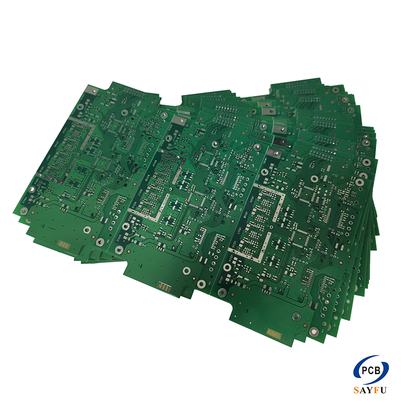
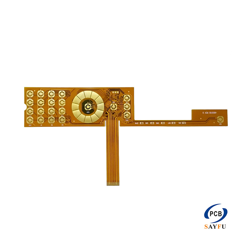
Printed circuit board production can be divided into two categories according to whether the substrate used is rigid or flexible: rigid printed boards and flexible printed boards. According to the number of layers of conductor patterns, it can be divided into single-sided, double-sided and multi-layer printed boards.
A printed board in which the entire outer surface of the conductor pattern and the surface of the substrate are on the same plane is called a flat printed board.
For terms and definitions of printed circuit boards, please refer to the national standard GB/T2036-94 “Printed Circuit Terminology”.
After the electronic equipment adopts the printed board, due to the consistency of the same type of printed board, the error of manual wiring is avoided, and the automatic insertion or mounting of electronic components, automatic soldering, and automatic detection can be realized, which ensures the quality of the electronic equipment. , improve labor productivity, reduce costs, and facilitate maintenance.
Printed boards have developed from single-layer to double-sided, multi-layer and flexible, and still maintain their respective development trends. Due to the continuous development in the direction of high precision, high density and high reliability, continuous reduction in size, cost reduction and performance improvement, printed boards will still maintain strong vitality in the future development of electronic equipment.
The mark of the technical level of the printed board
The mark of the technical level of the printed board For double-sided and multi-hole metallized printed boards: both in mass-produced double-sided metallized printed boards, two on the intersection of the 2.50 or 2.54mm standard grid Between the pads, the number of wires that can be routed is used as a sign.
A wire is arranged between the two pads, which is a low-density printed board, and the wire width is greater than 0.3mm. Two wires are arranged between the two pads, which is a medium density printed board, and the wire width is about 0.2mm. 1-0.15mm. Three wires are arranged between the two pads, which is a high-density printed board, and the wire width is about 0.1-0.15mm. Arrange four wires between the two pads, which can be considered as an ultra-high density printed board, with a line width of 0.05–0.08mm.