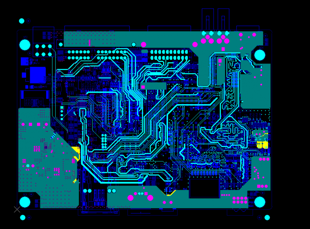
The design of the printed circuit board is based on the circuit schematic diagram to realize the functions required by the circuit designer. The design of the printed circuit board mainly refers to the layout design, and the layout of external connections needs to be considered. Various factors such as optimal layout of internal electronic components, optimal layout of metal connections and vias, electromagnetic protection, heat dissipation, etc. Excellent layout design can save production costs and achieve good circuit performance and heat dissipation performance. Simple layout design can be realized by hand, and complex layout design needs to be realized by computer-aided design (CAD).
In high-speed design, the characteristic impedance of controlled impedance boards and lines is one of the most important and common problems. First understand the definition of a transmission line: A transmission line consists of two conductors of a certain length, one for sending a signal and the other for receiving a signal (remember the concept of “loop” instead of “ground”). In a multilayer board, each trace is part of a transmission line, and the adjacent reference plane can act as a second trace or return. The key to a line being a “good” transmission line is to keep its characteristic impedance constant throughout the line.
The key to making a circuit board a “controlled impedance board” is to make the characteristic impedance of all lines meet a specified value, usually between 25 ohms and 70 ohms. In a multilayer circuit board, the key to good transmission line performance is to keep its characteristic impedance constant throughout the line.
But what exactly is characteristic impedance? The easiest way to understand characteristic impedance is to see what the signal encounters in transmission. This is similar to microwave transmission as shown in Figure 1 when moving along a transmission line of the same cross-section. Suppose a 1 volt voltage step wave is applied to this transmission line, such as connecting a 1 volt battery to the front end of the transmission line (which is located between the sending line and the return), once connected, this voltage wave signal travels along the line at the speed of light Propagation, it typically travels at about 6 inches/ns. Of course, this signal is indeed the voltage difference between the transmit line and the loop, which can be measured from any point on the transmit line and an adjacent point on the loop. FIG. 2 is a schematic diagram of the transmission of the voltage signal.
Zen’s approach is to “generate a signal” and then travel along this transmission line at 6 inches/ns. The first 0.01 nanoseconds advance by 0.06 inches, at which point the sending line has excess positive charge, and the loop has excess negative charge, and it is these two charge differences that maintain the 1 volt voltage difference between these two conductors, The two conductors in turn form a capacitor.
In the next 0.01 nanoseconds, the voltage of a 0.06-inch transmission line is adjusted from 0 to 1 volt, which must add some positive charge to the transmit line and some negative charge to the receive line. For every 0.06 inches of movement, more positive charge must be added to the transmit line and more negative charge must be added to the loop. Every 0.01 nanoseconds, another segment of the transmission line must be charged, and the signal then begins to travel along that segment. The charge comes from a battery at the front of the transmission line, and as it travels along the line, it charges successive sections of the transmission line, creating a 1-volt voltage difference between the sending line and the return. Every 0.01 nanoseconds advance, some charge (±Q) is obtained from the battery, and a constant amount of charge (±Q) flowing from the battery for a constant time interval (±t) is a constant current. The negative current flowing into the loop is actually equal to the positive current flowing out, and just at the front end of the signal wave, the AC current passes through the capacitors formed by the upper and lower lines, ending the entire cycle process.