Analysis of the concept and process requirements of PCB solder mask opening
Solder mask layer concept:
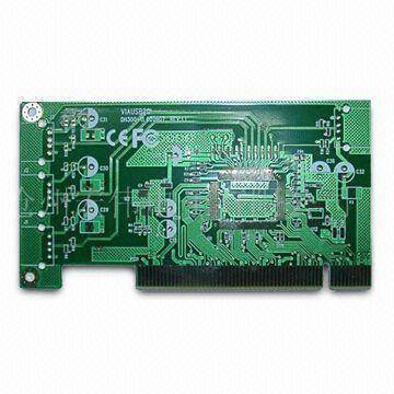
Solder mask layer refers to the part of the printed circuit board to be coated with green oil. In fact, this solder mask layer uses a negative output, so after the shape of the solder mask layer is mapped onto the board, it is not green oil solder mask, but the copper skin is exposed
Process requirements of solder mask:
The role of solder mask in controlling soldering defects during the reflow soldering process is important, PCB designers should minimize the spacing or air gaps around the pad features
Understanding the opening of PCB solder mask layer:
Solder mask opening refers to the size of the part where the copper needs to be exposed at the welding position, that is, the size of the part that does not cover the ink, and the cover line refers to the size and how much the solder mask covers the circuit part. If the distance between the covered wires is too small, the exposed wires will be caused during the production process.
Reasons for opening the PCB solder mask layer:
1. Aperture window: because many customers do not need ink plug holes, if the window is not opened, the ink will enter the hole. (This is for small holes) If the large hole is plugged with ink, the customer can’t press the key. In addition, if it is a gold plate, it must also open the window. 2. When soldering the PCB, the window will be opened with the PAD (that is, copper) of the solder paste layer: the customer needs welding and surface treatment.