PBGA (Plastic Ball Grid Array)
Images
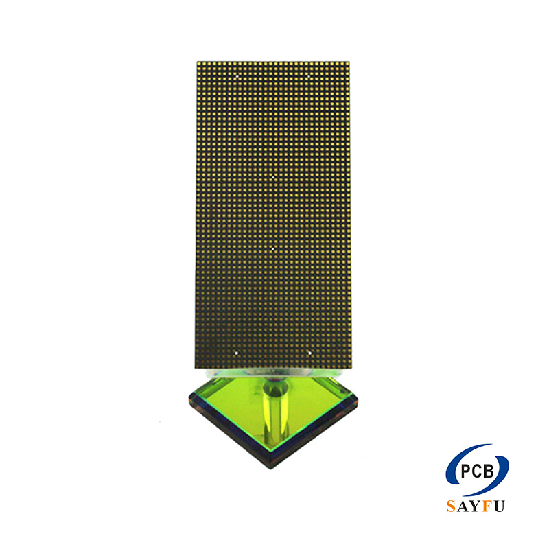
General Specification:
Number of layers: 4 layers (mainly), there are also designs with more than 6 layers
Structural features: There are many through-hole structures, the middle layer is mostly a copper layer, resin (main) or solder mask
Size: 1717mm~37.537.5mm
Board thickness: 0.4~0.6mm
Line width/line distance: 30/30 ~ 60/60 um
Gold finger spacing: 100~140 um
Surface treatment: Soft Au \ ENEPIG
Special process: TLP
DEFINE
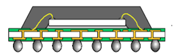
PBGA board: This kind of IC Substrate performs well in thermal dissipation and electrical performance and can dramatically increase chip pins. Ball grid array package substrate based on polymer plastic. Compared with QFP and other pin package forms, it has a larger number of I/O pins and higher reliability.
APPLICATION OF PBGA BOARD
PC Chipsets (Personal Computer Chipsets)
ASIC (Application Specific Integrated Circuit)
DSPs and memory
Microprocessor/controller/graphics processor
IC substrate PCBs are mainly applied on electronic products with light weight, thinness and advancing functions, such as smart phones, laptop, tablet PC and network in fields of telecommunications, medical care, industrial control, aerospace and military.
Rigid PCBs have followed through a series of innovations from multilayer PCB, traditional HDI PCBs, SLP (substrate-like PCB) to IC substrate PCBs. SLP is just a type of rigid PCBs with similar fabrication process approximately semiconductor scale.
IC substrate is a type of base board used to package bare IC (integrate circuit) chip. Connecting chip and circuit board, IC belongs to an intermediate product with the following functions:
• it captures semiconductor IC chip;
• there’s routing inside to connect chip and PCB;
• it can protect, reinforce and support IC chip, providing thermal dissipation tunnel.
Sayfu has been gradually growing up to a company that can fabricate IC Substrate. We are focuse on quality, cost, service, and experience continual development. If you have any ICS-projects, send us freely, we can quote to you early. Cantact eamil: [email protected]. A special circuit board for chip packaging. Similar to the traditional rigid PCB processing technology. But the smaller in size, thinner than PCB. ICS denser through holes, and finer than the traditional rigid PCB.