There are single-sided, double-sided, and multilayer PCBs. For simple appliances such as radios, single-sided PCBs are sufficient. However, with the progress of the times, electronic products need to be replaced, whether in terms of function or volume. For multi-functional, small-sized electronic products, both single-sided and double-sided PCBs cannot fully meet the requirements, and multi-layer PCBs must be used
Multilayer PCBs have many advantages, such as: high assembly density and small size; shortened wiring between electronic components, fast signal transmission speed, convenient wiring; good shielding effect, etc. There is no limit to the number of layers of multilayer boards. Currently, there are more than 100 layers of PCBs. Four and six layers are common.
When designing a multi-layer board, each layer should be kept symmetrical, and preferably even copper layers. If it is asymmetric, it is easy to cause distortion. Multilayer board wiring is performed according to the circuit function. In the outer layer wiring, more wiring is required on the soldering surface and less wiring on the component surface, which is beneficial to the maintenance and troubleshooting of the printed board. In terms of wiring, the power layer, ground layer, and signal layer need to be separated to reduce interference between power, ground, and signals. The lines of two adjacent layers of printed boards should be as perpendicular to each other as possible, or oblique lines and curves, not parallel lines, to reduce the interlayer coupling and interference of the substrate
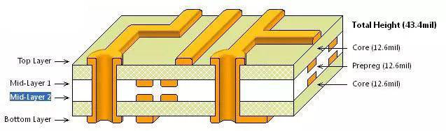
Compared to single-sided and double-sided PCBs, which layers are composed of multi-layer PCBs, what does each layer represent and what is its use? Multi-layer PCBs are mainly composed of the following layers: Signal Layers, InternalPlanes, Mechanical Layers, Masks, Silkscreen, and System
The signal layer is divided into a top layer, a middle layer, and a bottom layer, and is mainly used for placing various components, or for wiring and soldering. The internal power plane is also called the internal electrical plane and is dedicated to laying power and ground wires. The mechanical layer is generally used to place indicative information about the board making and assembly methods, such as the physical dimensions of the circuit board, data data, and via information. The solder mask also has a top layer and a bottom layer, and the pads or other objects placed on this layer are copper-free areas. The silk screen layer is mainly used to draw the outline of the component, the number of the placed component or other text information, and the system working layer is used to display the information that violates the design rules