PCB design is the most important key: Modern PCBs are not just time killers, they are also critical components with precise design requirements; the operating frequencies and signal rise/fall times of electronic devices are getting faster and faster, so PCBs have become increasingly important. Take a look at the following small stories that actually happened and you will get some inspiration.
PCB design A story about a PC motherboard
In 1985, PC chipsets had a 33MHz bus; Massa got a call from a local PC motherboard manufacturer at the time saying their new motherboard wouldn’t move. The IC supplier’s reference design worked, but the company made custom product outlines; and Massa noticed that their routing between components resulted in a lot of sharp angles in the PCB traces.
He also found that several critical signals were placed in large loops, and the board also had many vias; those small holes were to allow traces to go from the front of the board to the back. The company said their PCBs were designed by someone in Colorado, USA, cheap and fast, taking only one or two days to complete. Massa politely told them that the wiring was actually done with an automated software tool, so a board running a 33MHz signal would never work successfully.
Automatic routing tools are prone to errors. Early PCB software can only ensure the current connection of the signal to the pin, and does not consider the need for short traces for high-speed signals. The required vias should be laid out first, or because of vias, line widths The impedance mismatch caused by the change and so on will eventually lead to the failure of the entire PCB design.
A story about video chips
In 1995, I had an old brother who was working for a video chip company and had the same situation as before – the reference design was fine, but they had a big customer in Taiwan complaining that their chip wouldn’t work on the new PCB ; And the PCB design also has similar wiring errors.
The video chip company was faced with two choices, one was to frankly point out that the customer’s design had a problem and ask them to redo it, and the other was to make their own video chip a cheap metal mask modification to compensate for the customer’s poor PCB layout; later They opted for the second option, and of course the customer was happy, felt they were always right, and was happy with the customer service from the video chip company that sent them a new chip that worked without a hitch.
My friend said that this is a smart strategy for a semiconductor company; IC companies should import IP for their own chips, rather than spend money to teach their customers how to design. You can make changes within the chip and in turn collect money from the customer.
A story about the F-16 fighter jet
The author has been involved in the design of the radar jamming device of the F-16 fighter jet, and learned about the systematic PCB problems that some companies may also encounter; circuit board routing is considered a mechanical engineering task, so our electronic engineer threw out the circuit diagram and let other departments Do the circuit board wiring work.
The board I got had a very high-speed Emit-Coupled Logic (ECL) oscillator, but the 8-layer board prototype didn’t work; with so much board space, I’m wondering how on earth they got the design going smashed. It turned out that the mechanical engineers placed the components according to their shape in order to simplify the design of the aluminum heatsink below all the parts; the ECL chip was on the top left of the board, the resistors were placed in the center, and the crystal oscillator was on the right The lower corner, a full 8 muscles away from the ECL chip.
Since then we’ve made sure that the mechanical engineer has an electrical engineer sitting next to the component placement on the PCB, and that the entire layout is reviewed before it’s ready for manufacture (Figure 2).
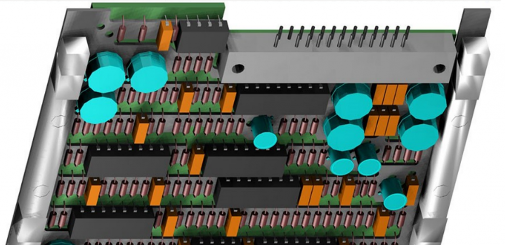
Figure 2 The PCB of the radar jamming device of the F-16 fighter jet. There is an aluminum heat sink under all the components; do not let the mechanical engineer lay out the PCB for the design of the heat sink, so as not to sacrifice the electronic energy.
A story about a power supply
When I was a consultant for HP in 1998, I used a Linear SEPIC converter chip, the LT1513IR, in my design; I looked at the product spec sheet and talked to the Linear application engineer Jon Dutra who approached me Say, the wiring diagram in their company’s spec sheet is wrong. Okay… stop laughing, I was young and a little stupid.
Dutra, who has now moved to Microsoft, patiently looked at the application example section of the spec sheet and explained why they suggested deploying the converter that way. I have a few good friends who are retired from Linear and they all assure me that many customers are loyal users of the company’s components because their application engineering support can help customers turn a wrong design into a right one; and I deployed the SEPIC in the way Linear suggested, and it worked the first time around (Figure 3).
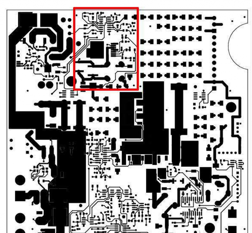
Figure 3 This is the PCB of the automatic test equipment, and because of the prior knowledge of the SEPIC converter (marked in red), my design worked the first time.
To learn more about PCB design know-how
There are many training courses and technical seminars you can attend. Professional senior engineers will teach you how to properly use component layout and routing rules to make your design avoid noise or be sensitive to noise; you You can also learn to ensure your designs have good signal and power integrity.
If you don’t want your product design to be messy or full of problems, you absolutely need to learn all about PCB design and manufacturing, which is the foundation of your product design, just like the foundation of a house, no one wants to It wobbles!