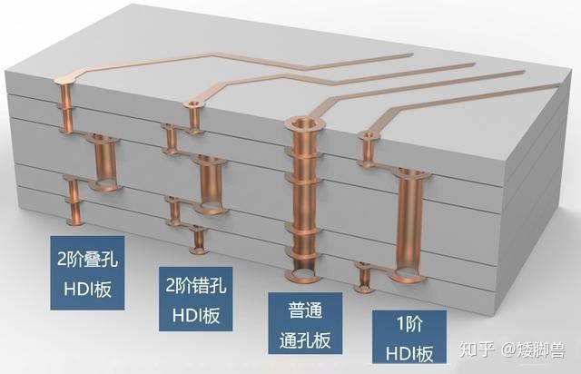
Via-connection channel of double-layer board
This is the most confusing part before. When you get a PCB, you will find that there are many small holes with the size of the needle tip. This is the via. Its structure is as follows.
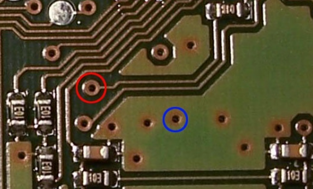
The function of the vias is mainly to connect the copper wires on the front and back of the board. Most of the vias are the red areas in the figure. When the front wires are not well arranged due to staggering, the vias can be used. Like an “overpass”, it converts the two-dimensional plane wiring into a three-dimensional space. The vias in the blue area are mainly to connect the front and back copper plates to achieve the effect of “common ground”.
The figure below clearly shows the structure of the via, and the copper in the hole is generally obtained by electrolytic reduction.
Pads – can actually be used to identify positive and negative electrodes
Pads are used for soldering component pins. Its size is larger than vias. Interestingly, the pads are not only round, but also square. Generally, square pads represent high-voltage pins.
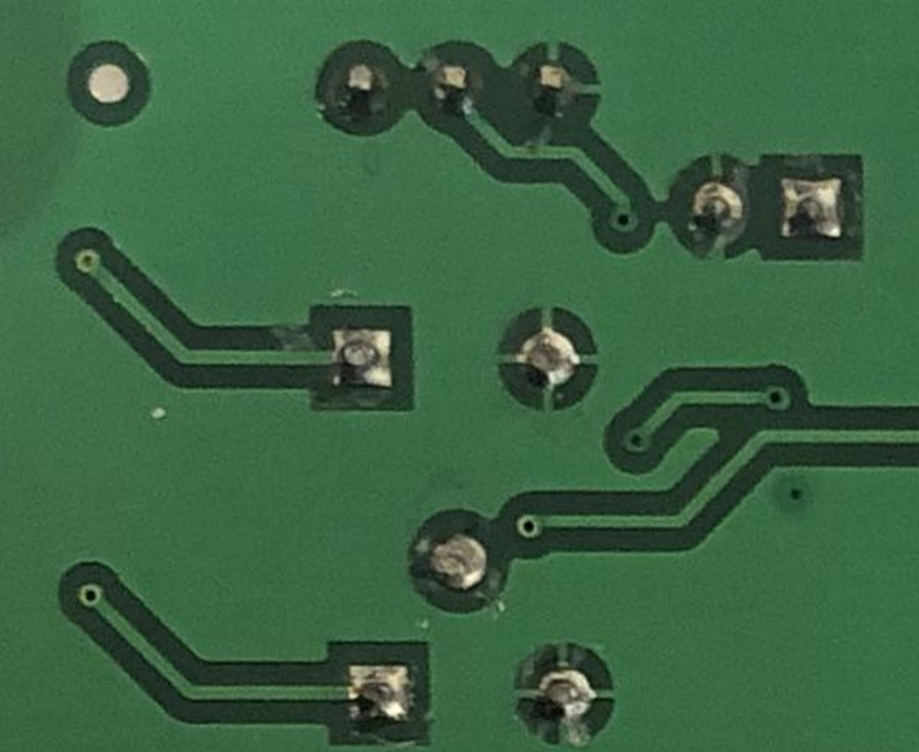
Another small detail in the above picture is that some circular pads are cross-shaped, which directly grounds the pins. The ground on the PCB is actually connected to the negative electrode, and the large-area copper plate is connected to the negative electrode of the power supply .This ensures that all GND pins are in common ground.
Commonly used electronic components
The most commonly used resistors are not shown in the picture, and now the chip resistors are mainly used, and there are few in-line resistors.
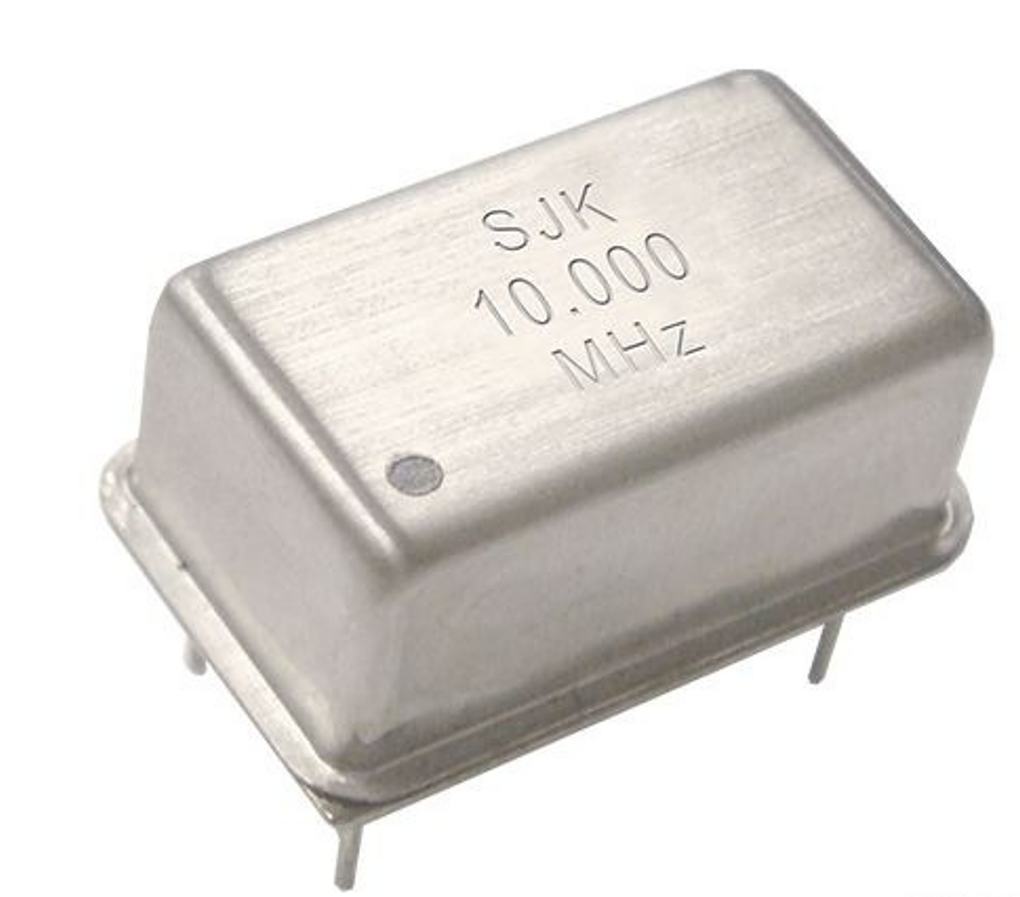
Crystal Oscillator – the heart of the circuit board, the numbers above represent the frequency.
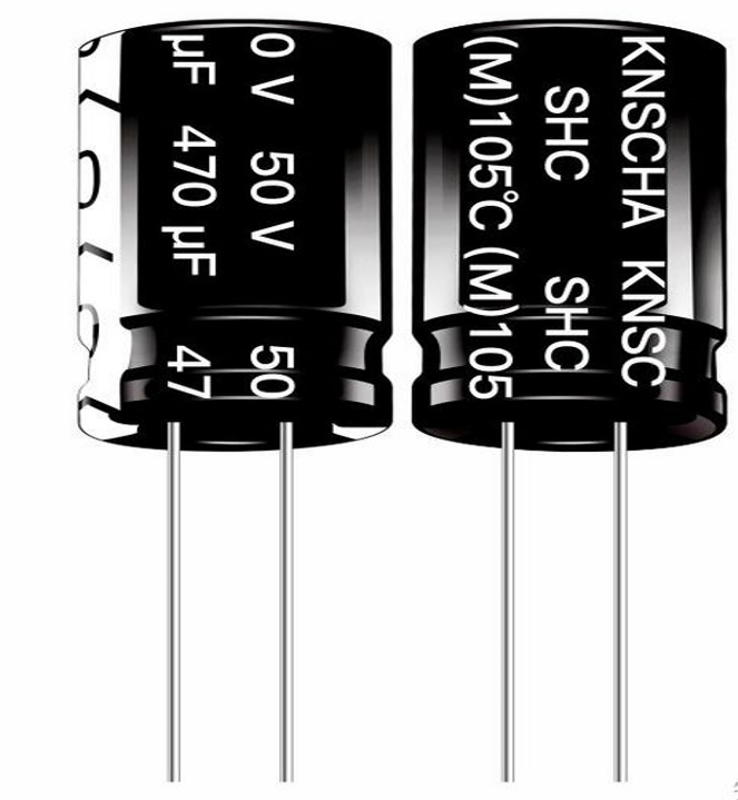
Capacitors, either black cylindrical or flat.
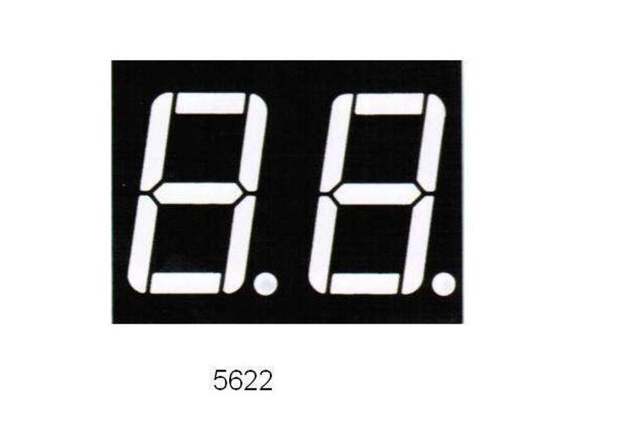
Digital tube, of course, many now use the display directly
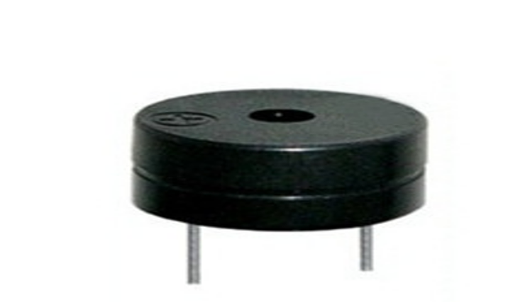
Buzzer
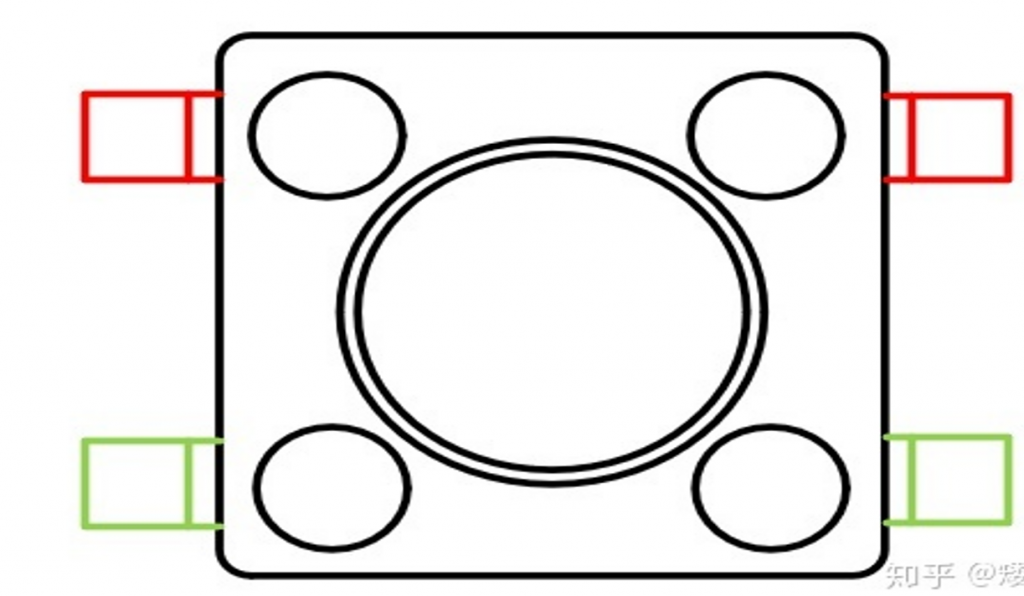
Four-pin switch – the pins of the same color in the picture are connected.
PCB package
The so-called PCB packaging is to express the actual electronic components, chips and other parameters (such as component size, length and width, pin spacing, etc.) in the form of pictures, so that they can be called when drawing PCB diagrams.
PCB sub-assembly is distinguished according to the installation method, which can be divided into SMD devices, plug-in devices, and special devices (sinking board devices)
Silkscreen – let’s engrave the name
After designing a PCB board, and finally put your name and studio logo on the finished product, the satisfaction is overwhelming. Of course, the main function of silk screen printing is to indicate the corresponding component labels. After the PCB is designed, you can use a piece of A4 paper Print it out and put the components on it to see if there is any obstruction and if the font size is appropriate. The common logos are:
R(resistance) resistance
U(unit) unit module/integrated circuit
C (capacitance) capacitance
Q tertiary tube
X crystal oscillator
Conclusion of PCB board
Personally, everyone who uses PCB should learn about PCB making, including circuit design, AltiumDesign/Protel, soldering circuit boards, etc. Maybe you will never need to make a circuit board yourself, but having this knowledge can make you get familiar with the circuit of the board faster and get ready for programming.