HDI Mobile phone PCB is a compact product designed for small volume users. It adopts modular parallel design, a module capacity of 1000VA (height 1U), natural cooling, can be directly placed in a 19 “rack, up to 6 modules in parallel. The product adopts full digital signal process control (DSP) technology and a number of patented technologies, with full range of load adaptability and strong short-term overload capacity, can not consider the load power factor and peak factor.
General Specification
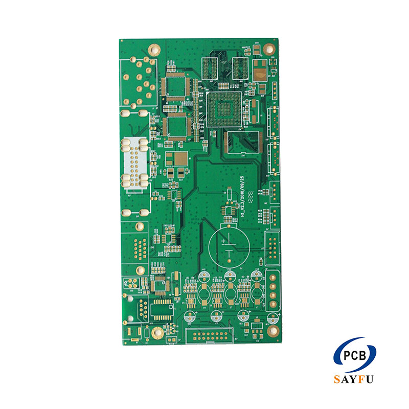
| Unit siz | 95*50mm |
| Material | FR4 IT180A |
| Finished Thickess | 1.6mm |
| Finished Copper | Inner35um/Outer70um |
| Surface treatment | ENIG |
| Soldermask | Green soldermask |
| Line/space | 3mil/3mil |
| Impedance control | differential 90 & 100ohm / 3 impedance control values |
| Special Technology | Buried Blind vias /resin plugged |
HDI stands for High Density Interconnector. It is a type of printed board that uses micro-blind buried hole technology to produce a circuit board with High circuit distribution Density. HDI is a compact product designed for small volume users. It adopts modular parallel design, a module capacity of 1000VA (height 1U), natural cooling, can be directly placed in a 19 “rack, up to 6 modules in parallel. The product adopts full digital signal process control (DSP) technology and a number of patented technologies, with full range of load adaptability and strong short-term overload capacity, can not consider the load power factor and peak factor.
Electronic design is constantly improving the performance of the whole machine, but also trying to reduce its size. From mobile phones to smart weapons, “small” is a constant pursuit. High density integration (HDI) technology enables end product designs to be miniaturized while meeting higher standards of electronic performance and efficiency. HDI is widely used in mobile phones, digital cameras, MP3, MP4, notebook computers, automotive electronics and other digital products, among which mobile phones are the most widely used. HDI board is generally manufactured by build-up method. The more times of stacking, the higher the technical level of the board. Ordinary HDI board is basically one layer, high order HDI uses two or more layers of technology, at the same time the use of stacking holes, electroplating hole filling, laser direct drilling and other advanced PCB technology. Advanced HDI boards are mainly used in 3G mobile phones, advanced digital cameras, IC boards, etc.
Development prospects: According to the use of high-order HDI board –3G board or IC board, its future growth is very rapid: in the next few years, the growth of 3G mobile phones in the world will exceed 30%, China will soon issue 3G licenses; Prismark, an IC board industry consultancy, predicts that China will grow by 80% from 2005 to 2010, which represents the direction of PCB technology development.
HDI Mobile phone PCB advantages
PCB cost reduction: When PCB density increases beyond eight layers, the cost of manufacturing with HDI is lower than that of the traditional complex laminating process.
Increased circuit density: Interconnections between traditional circuit boards and components
It is conducive to the use of advanced construction technology
Have better electrical performance and signal correctness
Good reliability
Can improve thermal properties
Improve RF/ELECTROMAGNETIC interference/electrostatic release (RFI/EMI/ESD)
Increase design efficiency