The PCB assembly process is a precise and multi-stage process that transforms a bare board into a functional electronic circuit. This journey from components to a finished board is critical to the production of virtually all modern electronics.
The process begins with Solder Paste Printing.
We place a stencil, laser-cut to match the board’s solder pad layout, over the PCB. We spread the solder paste, a mixture of tiny solder spheres and flux, across the stencil. And depositing a precise amount of paste onto each pad where components will sit.
Next comes Component Placement.
In modern manufacturing, this is primarily performed by high-speed, automated machines called Pick-and-Place robots. These machines use vacuum nozzles to pick up Surface Mount Devices (SMDs) from reels or trays. And place them accurately onto the solder-pasted pads. The tackiness of the paste holds the components in place temporarily.
The third stage is Reflow Soldering
This step permanently attaches the SMDs. The assembled board travels through a reflow oven on a conveyor belt. The oven subjects the board to a carefully controlled temperature profile, first heating the board to activate the flux, then reaching a peak temperature to melt the solder, and finally cooling it to form solid, reliable electrical connections.
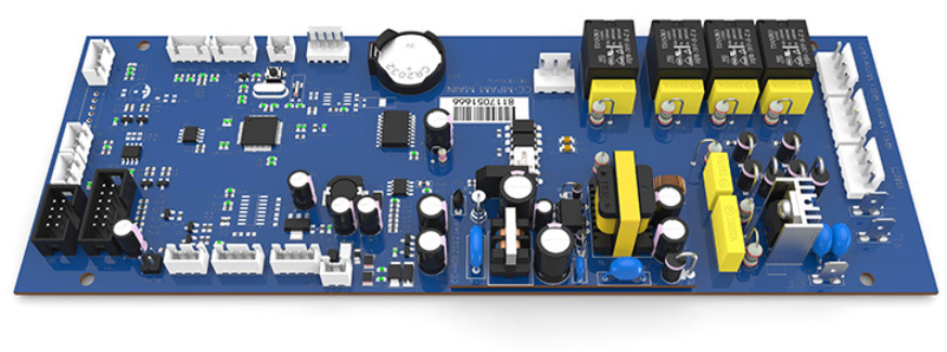
For boards that also contain through-hole components, we require an additional step: Through-Hole Insertion and Soldering. We can do this manually for low-volume projects or using automated insertion machines. We achieve the soldering typically via Wave Soldering, where the bottom side of the board passes over a wave of molten solder. Which wicks up to the leads and pads, creating strong mechanical and electrical bonds.
Inspection and Testing
Finally, the process concludes with Inspection and Testing. Automated Optical Inspection (AOI) systems use cameras to check for common defects like misaligned components or solder bridges. For more complex validation, boards may undergo In-Circuit Testing (ICT) or Functional Testing (FCT) to verify electrical performance and ensure the assembly operates as designed.
In summary, the PCB assembly process is a sophisticated symphony of automation and precision, ensuring that the final product is reliable, efficient, and ready for its intended application.