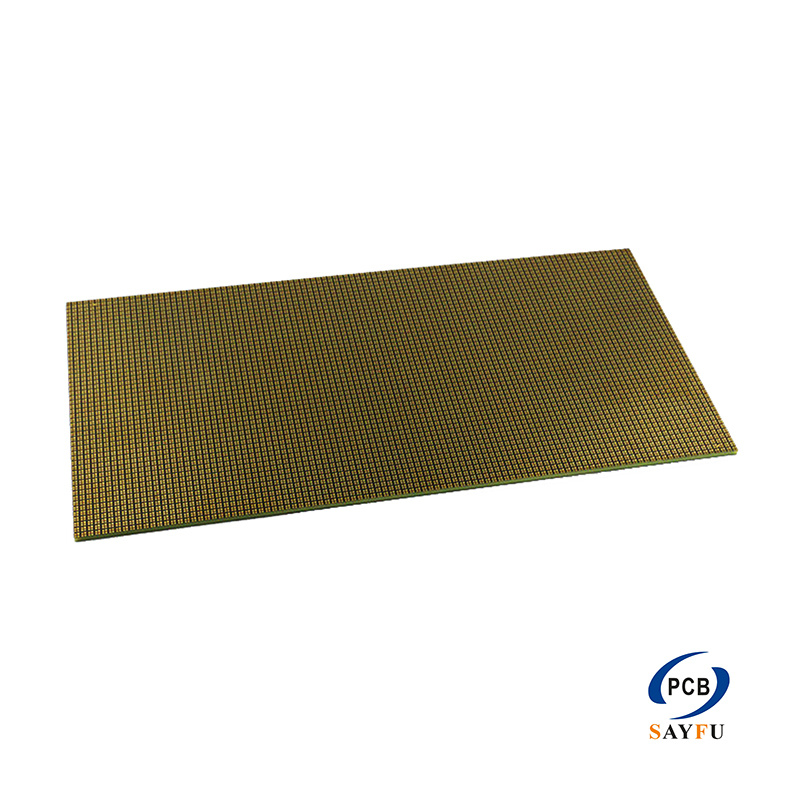
MCP(Multi-Chip Package)
Images

General Specification:
Number of layers: 2 layers
Structural features: more blind hole filling structures
Size: 12*14mm
Board thickness: 0.2~0.3mm
Line width/line distance: 25/25 um
Gold finger spacing:
Surface treatment: OSP
Special process: VIP
DEFINE
MCM IC Substrate. MCM is an abbreviated form of multi-chip module. This type of IC substrate absorbs chips with different functions into one package. As a result, the product can be an optimal solution due to its attributes including lightness, thinness, shortness and miniaturization. Naturally, since multiple chips are packaged into one package, this type of substrate doesn’t perform so well in signal interference, thermal dissipation, fine routing etc.

APPLICATION
Smartphone memory
Multimedia processor
Other mobile electronic device storage
IC substrate PCBs are mainly applied on electronic products with light weight, thinness and advancing functions, such as smart phones, laptop, tablet PC and network in fields of telecommunications, medical care, industrial control, aerospace and military.
Rigid PCBs have followed through a series of innovations from multilayer PCB, traditional HDI PCBs, SLP (substrate-like PCB) to IC substrate PCBs. SLP is just a type of rigid PCBs with similar fabrication process approximately semiconductor scale.
CSP is a chip-scale package, it is not a separate form of packaging, but a chip-scale package called when the chip area is comparable to the package area. The CSP package allows the ratio of chip area to package area to exceed 1:1.14, which is quite close to the ideal situation of 1:1, which is about 1/3 of the ordinary BGA; the center pin form of the CSP package chip is effectively shortened The signal conduction distance reduces its attenuation, and the anti-interference and anti-noise performance of the chip can also be greatly improved. In the CSP packaging method, the chip particles are soldered on the PCB board through solder balls. The PCB board has a large contact area, so the heat generated by the chip in operation can be easily conducted to the PCB board and dissipated.
Development prospects: Chip-scale packaging developed in response to the light, thin, short and small electronic products is a new generation of packaging methods. According to the development trend of electronic products, chip-scale packaging will continue to develop rapidly and gradually replace TSOP (ThinSmallOutlinePackage) packaging and Ordinary BGA package.