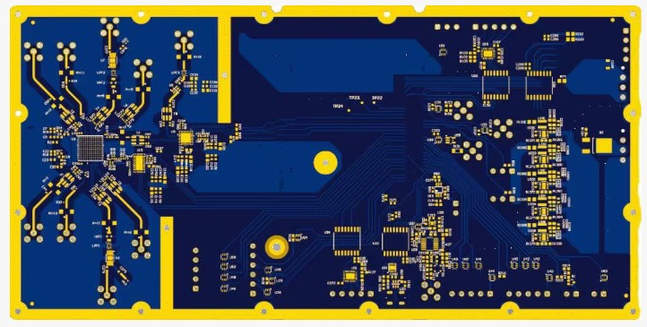
High speed PCB design is a critical discipline in modern electronics, directly impacting the performance and reliability of advanced devices. This specialized field focuses on managing signal integrity, power distribution, and electromagnetic interference in circuits where signal frequencies are so high that the physical layout itself influences functionality. Success in this area requires a deep understanding of both theoretical principles and practical implementation strategies.
Core Principles of Operation for High Speed PCB
The foundation of any successful high-speed board lies in managing signal integrity. Consequently, controlled impedance routing is essential to prevent signal reflections. Furthermore, proper grounding schemes and the use of differential pairs help minimize noise and crosstalk. Therefore, designers must carefully plan the stack-up and material selection from the very beginning to meet the electrical requirements.
Power Integrity Considerations
Moreover, a stable power supply is equally vital. As switching speeds increase, the power distribution network, or PDN, must provide clean and stable voltage. This is achieved by using a combination of decoupling capacitors placed strategically across the board. Additionally, careful plane design helps create a low-impedance path for power, ensuring that the entire high speed PCB functions without voltage fluctuations that could cause errors.
Addressing Signal Integrity of High Speed PCB
Another major challenge is maintaining signal quality from transmitter to receiver. To achieve this, traces must be routed to avoid sharp bends, which can cause impedance discontinuities. Likewise, the use of termination resistors is often necessary to absorb signal energy and prevent ringing. For instance, careful simulation throughout the design process is crucial for predicting and correcting potential signal integrity issues before manufacturing.
Advanced Routing Techniques
Finally, effective routing strategies bring everything together. A key practice is to route critical high-speed signals on adjacent layers with a reference plane between them for shielding. Also, length matching between related signals is mandatory to ensure synchronous arrival. In summary, mastering these advanced techniques is fundamental for creating a robust and reliable high speed PCB that meets all performance specifications in demanding applications.