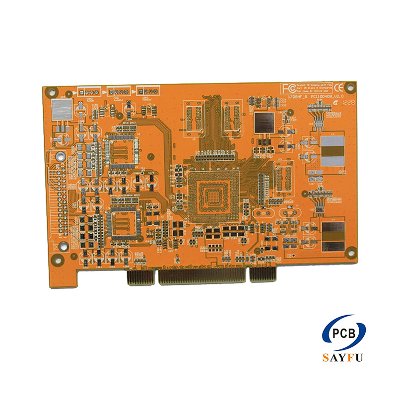
The Critical Role of HDI(High-Density Interconnect) in Advanced AI Technology
With the rapid development of artificial intelligence (AI), HDI(High-Density Interconnect) (PCBs)—often termed the “neural network” of electronic devices—directly determine the computational power release, data transmission efficiency, and stability of AI systems. In AI chips, servers, edge computing devices, and terminal equipment, HDI(High-Density Interconnect) enables efficient AI deployment and performance breakthroughs material innovation, structural design, and process upgrades.
High-Density Interconnect (HDI) Technology Empowers AI Computing
The high computational demands of AI chips drive HDI(High-Density Interconnect) toward higher integration density. HDI technology utilizes ultra-fine circuits (line width down to 25μm) and micro-vias (diameter below 50μm), increasing wiring density by 5× compared to conventional PCBs and significantly shortening signal transmission paths. For instance, in Transformer-architecture chips, HDI substrates reduce data latency by 30%, enabling an additional 30 billion data exchanges per second. Moreover, multi-layer power supply designs and embedded resistor-capacitor technologies confine power supply ripple within ±2%, supporting stable 100A instantaneous current output for AI chips without computational fluctuations.
High-Frequency Signal Transmission and Thermal Optimization
5G-AI convergence scenarios require HDI(High-Density Interconnect) to balance high-frequency signal integrity and thermal management. Ceramic-filled substrates (Dk=3.0±0.05) and low-roughness circuit processes reduce millimeter-wave (28GHz) signal loss by 45% and optimize reflection coefficients to -30dB, ensuring distortion-free 10Gbps data transmission. For heat dissipation, copper-based substrates with embedded vapor chambers achieve thermal conductivity of 5W/(m·K), lowering chip junction temperatures by 20°C and maintaining stability during sustained high-load AI server operations.
Industrial-Grade Reliability and Smart Manufacturing
In industrial automation and edge computing, PCBs must withstand extreme conditions. High-heat-resistant substrates (Tg 180°C) and redundant signal pathways ensure 8,000 hours of failure-free operation within -40°C to 85°C environments, delivering 99.9% computational stability. Concurrently, AI-powered quality inspection systems leverage deep learning to reduce defect escape rates to near-zero while boosting production efficiency by 40%, accelerating the industry’s shift from “experience-driven” to “data-driven” paradigms.
Diversified Application Scenarios
From smart terminals (e.g., AI phones, AR glasses) to computing base stations and IoT gateways, HDI(High-Density Interconnect) technology is deeply embedded in the AI ecosystem. For example, in a smart agriculture project, optimized IoT gateway PCBs supported 200+ concurrent device connections, improving AI environmental prediction accuracy by 25%. Looking ahead, 3D IC technology will further break integration barriers, positioning PCBs as the cornerstone for AI systems targeting exa-scale computing (EFlops).
Keywords Highlights:
PCB: Printed Circuit Board (线路板)
HDI: High-Density Interconnect (高密度互连)
Tg: Glass Transition Temperature (玻璃化转变温度)
EFlops: Exa-FLOPS (百亿亿次浮点运算/秒)
