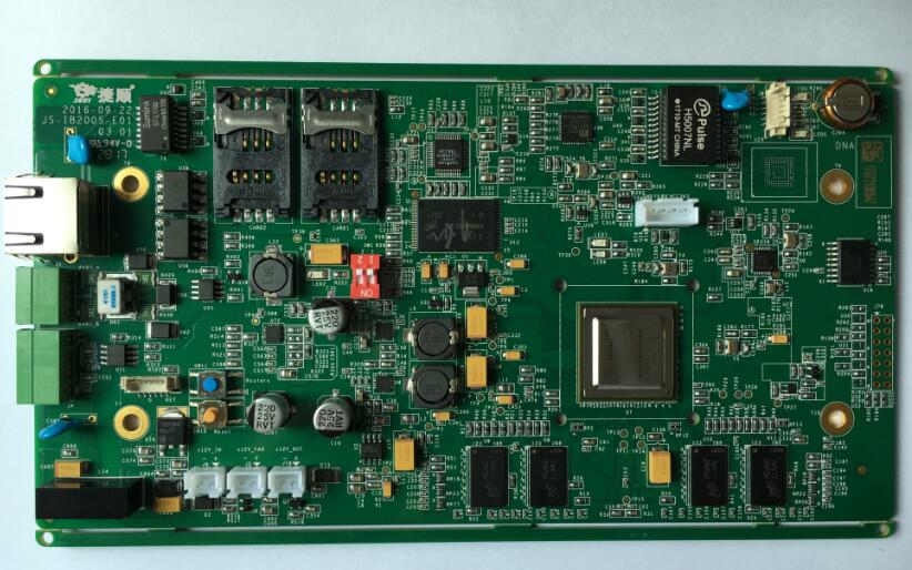
High Volume PCB Assembly refers to the process of large-scale printed circuit board assembly. It is a highly automated electronic manufacturing technology specifically designed for the efficient and rapid production of large quantities of electronic devices, such as smart phones, automotive electronics, and consumer products. This assembly method relies on advanced equipment, such as surface mounters, reflow ovens, and automatic optical inspection systems, to achieve high precision and consistency in production. In the global electronics industry, High Volume PCB Assembly has become a key link to meet market demands. Through standardized processes and large-scale operations, it significantly improves manufacturing efficiency while reducing unit costs. With the popularization of Internet of Things and 5G technologies, this assembly method is becoming increasingly important, helping enterprises cope with the highly competitive market environment.
The main advantages of High Volume PCB Assembly
High Volume PCB Assembly offers numerous significant advantages, making it the preferred choice in modern electronic manufacturing. Firstly, since High Volume PCB Assembly significantly reduces the unit production cost through economies of scale, the fixed investment and operating expenses are spread across a large number of products, thereby saving resources for the enterprise. Secondly, the automated process greatly enhances production efficiency, reduces human errors, and ensures the consistency and reliability of the products, such as in the component mounting and welding stages, where machines can operate with millimeter-level precision, avoiding common defects. Moreover, this assembly method supports a rapid transition from prototype to mass production, enabling enterprises to respond quickly to market changes and shorten the product launch time. Finally, strict quality control measures, such as automatic optical inspection and functional testing, ensure the high quality of the final products and reduce the return rate and maintenance costs.
Optimization and implementation of the production process
When conducting High Volume PCB Assembly, optimizing the production process is of utmost importance to ensure efficient and sustainable operations. Firstly, material management involves meticulous coordination of the supply chain to ensure a stable supply of key components such as chips and resistors, minimizing production disruptions caused by shortages. Then, the assembly process encompasses multiple steps, including solder paste printing, component mounting, reflow soldering, and cleaning. Each step must be strictly controlled by automated equipment to maintain a high yield rate. Finally, the quality inspection phase employs various testing methods, such as in-line testing and environmental stress screening, to identify and correct defects, ensuring that the products meet industry standards. Through this systematic approach, enterprises can not only enhance production efficiency but also adapt to changing market demands, achieving long-term growth.
