Custom PCB board,The Chinese translation is 定制印刷线路板.In simple terms, it is a circuit board that is specifically designed and manufactured according to your specific requirements, functions and specifications, rather than a generic PCB purchased from the market.
Over time, PCBs have become extremely advanced, and now any type of final requirement can be achieved through them. The key role of electronic circuits is to receive input, process it, and generate output that is useful for the application. Each circuit board represents a unique circuit and operates within the confines of its circuit characteristics. Therefore, due to their core design, the performance, application scope, and usage methods of circuit boards are all limited.
The existing users and terminal applications have higher requirements for the product, and they expect to obtain more functions from a single product. According to the usual practice, each unique function needs to be realized through a dedicated PCB. How to integrate all these printed circuit boards for a single project to produce a Custom PCB Board will inevitably result in a larger product that is more complex to use. To address these challenges, electronic designers have adopted the concept of custom design in the field of printed circuit board technology.
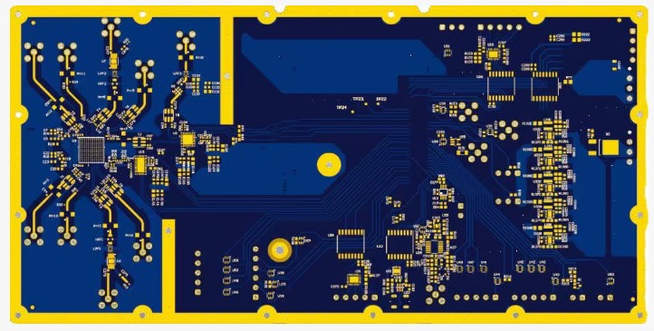
Custom PCB Board Layout Design
Once the core features of the product have been determined based on the needs of the end users, the design phase can begin. Draw a logic circuit diagram that includes all key, main and secondary elements. Use simulation tools to check if there are any errors, output changes or potential defects in the circuit. This is an important step in understanding how to manufacture custom printed circuit boards. Additionally, convert the schematic design of this printed circuit board into the actual layout of the printed circuit board.
Here, the layout will be adjusted based on the final PCB size and stack-up structure. Careful selection of the through-hole pads (PTH) or surface mount (SMD) packages for the PCB is necessary to meet the circuit specifications. The component layout, routing paths, width, length, spacing, clear printing, and all other key parameters must be handled meticulously. The final PCB design scheme, bill of materials (BOM), and manufacturing instructions should also be prepared in full for production reference. For sub-components, the connections between sub-components and the final assembly method must be correctly determined.
Summary
Due to the increasing demand for multiple functions in a single product and the continuous advancement of technology, custom PCB are becoming increasingly popular. With the latest software and automated manufacturing technologies, understanding how to produce custom PCB boards enables engineers to handle such complex projects in an accurate manner. The future of printed circuit boards will be more advanced and be able to meet the needs of more complex users.