Via-In-PAD is called The Micro Bridge on PCB. In today’s increasingly sophisticated landscape of high-speed digital circuits and RF systems. A technology known as “Via-In-PAD” has quietly emerged as a key solution for enhancing signal integrity. These minuscule channels, drilled directly into component pads, may appear simple at first glance. But they are, in fact, a bridge enabling modern electronic design to achieve higher performance.
1. Traditional PCB
While traditional PCBs place vias outside the pads—a mature process—this approach significantly increases parasitic inductance when handling high-speed signals, leading to signal reflection and attenuation. The via-in-pad technology revolutionizes this design by positioning vias precisely at the center of the pad. This provides the shortest transmission path for high-frequency signals. This subtle yet critical modification substantially reduces the risk of signal distortion, proving particularly invaluable for GHz-level RF signals and high-speed digital signals.
2. Challenges Faced by Via-in-PAD PCBs
However, mastering this technology is no simple feat. Via-in-pad presents a critical plating and filling challenge—it requires absolutely dense copper fill without voids. Any imperfection can trap volatiles, creating a high risk of board delamination (“popcorning”) during subsequent high-temperature assembly processes. Additionally, the “Solder Wicking” phenomenon must be precisely controlled during soldering to prevent molten solder from being drawn away from the joint through the via. Which would compromise connection reliability.
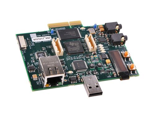
3. The Application of Via-In-PAD PCB
From the antenna modules of smartphones and high-speed processors in server motherboards to the precision sensing circuits of medical equipment, via-in-pad technology has become ubiquitous. It serves not only as a solution for space optimization but also as a critical foundation for ensuring performance.
As the demands for signal rates continue to escalate with the advent of 5G communication and AI computing. This “micro-art” of via-in-pad will continue to propel electronic devices toward higher frequencies, more compact form factors, and enhanced performance. It stands as an invisible pillar, supporting the information superhighway within the most confined of spaces.
Editor: Kevin Tian; Company: Sayfu Multilayer Circuits Co., Ltd.; Email: [email protected]