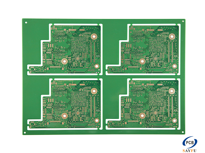
High-Density Interconnect HDI Boards are core carriers that meet the demands for miniaturization and high integration of electronic devices. Their structural design directly determines signal transmission efficiency and space utilization.
1. Basic Structural Features of High-Density Interconnect HDI Boards
The core features of HDI Boards center around “high density”.
- First, the line width and spacing are extremely small. The conventional line width and spacing can reach below 3mil/3mil, which is much lower than the 6mil/6mil standard that traditional PCBs adopt, thus allowing it to accommodate more circuits.
- We adopt a layered structure of “core board + build-up layers”. Second, we realize multi-layer wiring by stacking thin dielectric layers and conductive layers on both sides of the core board.
- Third, we use high-precision base materials. Therefore, we mostly apply low-loss materials such as FR-4 or high-frequency materials to reduce signal attenuation and adapt to high-speed transmission scenarios.
2. Via Structure Features of HDI Boards
Vias are key to realizing inter-layer interconnection in HDI Boards, and their structure has three major advantages.
- First, microvias are the core. Their diameter is usually below 0.15mm, which is only 1/3 of that of traditional through-holes, greatly saving board space.
- Second, we widely use blind vias and buried vias. Specifically, blind vias only connect the surface layer and inner layers, while buried vias hide between inner layers; furthermore, we avoid space waste that traditional through-holes cause by penetrating the entire board.
- Third,we adopt the “laser drilling + electroplating filling” process to achieve high-density arrangement of vias. Thereby reducing signal crosstalk and improving circuit stability.
3. Classification of High-Density Interconnect HDI Boards
HDI Boards are mainly classified by the number and distribution of vias.
- The first type is the 1+N+1 type. We stack one build-up layer on each side of the core board (N layers), and we only distribute vias between the surface layer and the core board.It is suitable for medium and low-density requirements.
- The second type is the 2+N+2 type. We stack two build-up layers on each side of the core board, and these layers support interconnection between the surface layer, sub-surface layer and core board. Manufacturers also adapt this structure to higher-density chip packaging.
- The third type is Any-Layer HDI (Any-Layer Interconnection). Microvias can directly connect all layers without relying on the core board. This type has the highest density currently and often finds application in devices such as 5G base stations and high-end servers.
Overall, the structural design of HDI Boards, specifically by reducing size and optimizing interconnection methods, ultimately provides key support for the development of electronic devices towards thinner, lighter and higher performance.