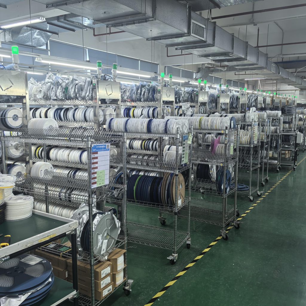
Rigid Flex Circuit Manufacturing is a sophisticated process that combines the techniques used for both traditional rigid PCBs and flexible circuits. It involves creating a multilayer board that integrates rigid sections for component support and flexible sections for dynamic bending. The basic fabrication process can be outlined in several key stages.
1.Material Preparation and Inner Layer Imaging for Rigid Flex Circuit Manufacturing:
The process begins with the selection of base materials: typically, polyimide for the flexible layers and FR-4 or similar for the rigid sections. The inner flexible copper layers are first cleaned and coated with a photosensitive film. Using precise laser direct imaging (LDI), the circuit pattern is exposed onto the film. The unexposed areas are then etched away, forming the intricate conductive pathways on the flexible inner layers.
2.Coverlay Lamination and Layer Bonding for Rigid Flex Circuit Manufacturing:
Instead of a solder mask, flexible circuits use a polyimide coverlay. This protective layer, pre-punched with openings for pads and vias, is laminated onto the patterned inner layers using a heat-activated adhesive. Multiple etched layers (flexible and rigid) are then precisely aligned and bonded together under high heat and pressure using pre-preg (pre-impregnated) bonding sheets to form a single multilayer structure.
3.Drilling and Plating
Once laminated, precision drills create through-holes that connect the different layers. This step is critical for creating electrical connections between the rigid and flexible sections. The holes are then chemically cleaned and coated with a thin layer of copper through an electro-less plating process, followed by a thicker electroplating step to ensure a reliable conductive barrel.
4.Outer Layer Processing and Final Finishes
The outer rigid layers are then processed similarly to the inner layers—imaged, etched, and stripped to define the outer circuitry. A solder mask is applied to the rigid areas to protect the copper traces, leaving component pads exposed. Finally, a surface finish (such as ENIG or HASL) is applied to the exposed pads to prevent oxidation and ensure solderability.
5. Contour Routing and Testing
The final and most distinctive step is the contour routing. Using precision CNC machines, the rigid panels are cut out, and the flexible sections are profiled, creating the final board outline and separating the rigid areas from the flexible ones. Each board undergoes rigorous electrical testing and visual inspection to ensure reliability before being shipped.
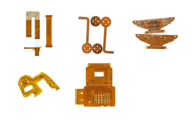
This intricate process results in a highly reliable, space-saving, and durable component essential for modern electronics like medical devices, aerospace systems, and consumer wearables.