PCB Materials, A Printed Circuit Board (PCB) is the foundational platform for virtually all modern electronics, from smThe Essential Building Blocks: Understanding Basic PCB Materials
A Printed Circuit Board (PCB) is the foundational platform for virtually all modern electronics, from smartphones to satellites. While its design is complex, its core construction relies on a surprisingly small group of essential materials. Understanding these basic components—the substrate, the conductive layer, the solder mask, and the silkscreen—is key to appreciating how these intricate boards function.
1.The Foundation: The Substrate (Laminate) for PCB Materials
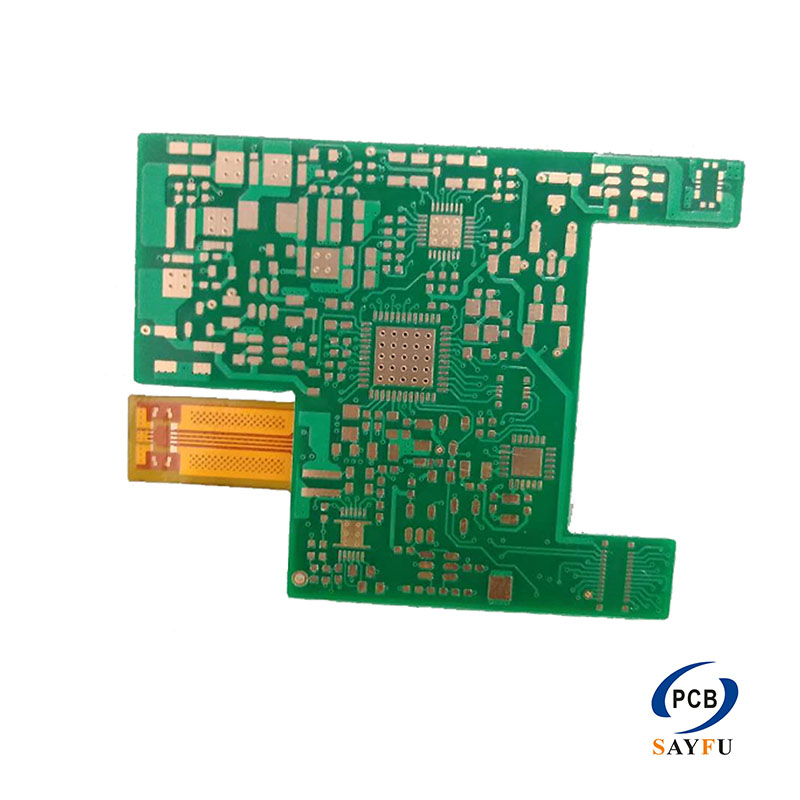
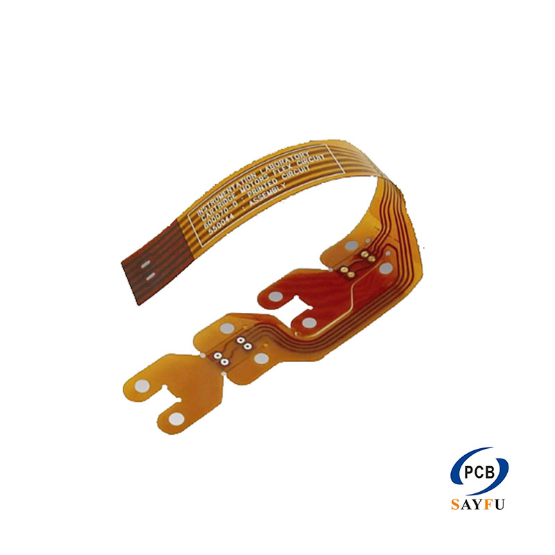
The heart of any PCB is the substrate, most commonly a material called FR-4. This glass-reinforced epoxy laminate is the workhorse of the industry, prized for its excellent strength-to-weight ratio, flame retardancy (the “FR” in its name), and good electrical insulation properties. For flexible circuits, a polyimide film is often used instead, allowing the board to bend and twist. In high-frequency applications, materials like PTFE (Teflon) are preferred for their superior dielectric properties. The substrate provides the rigid, insulating base upon which everything else is built, determining the board’s fundamental mechanical and thermal characteristics.
2.The Conductive Pathways: Copper for PCB Materials
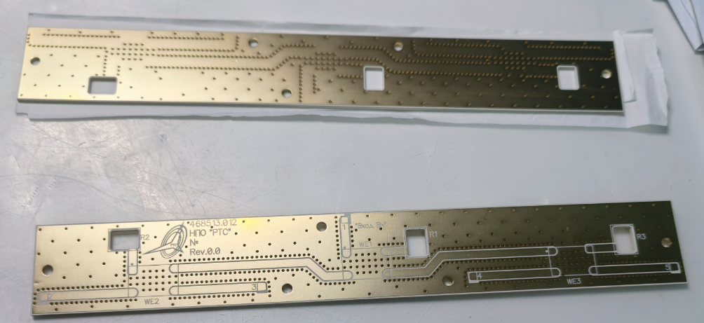
Once the substrate is prepared, a thin layer of copper is applied to one or both sides to form the electrical pathways, or traces. This is typically done through lamination or electroplating. The copper foil is etched away using a chemical process, leaving only the desired circuit pattern behind. The thickness of the copper layer is critical and is measured in ounces per square foot, directly impacting the amount of current the trace can carry. This intricate web of copper is what allows electrical signals and power to travel between components, forming the literal “circuit” in the board.
3.The Protective Coat: Solder Mask for PCB Materials
Once the substrate is prepared, a thin layer of copper is applied to one or both sides to form the electrical pathways, or traces. This is typically done through lamination or electroplating. The copper foil is etched away using a chemical process, leaving only the desired circuit pattern behind. The thickness of the copper layer is critical and is measured in ounces per square foot, directly impacting the amount of current the trace can carry. This intricate web of copper is what allows electrical signals and power to travel between components, forming the literal “circuit” in the board.
4.The Informative Layer: Silkscreen
The final touch is the silkscreen, the white (or other colored) lettering and symbols printed on the component side of the board. This non-conductive epoxy ink provides crucial information for assembly, testing, and repair. It typically includes component designators (like R1 for resistor 1), polarity indicators, pin-1 markers, and company logos. While not electrically functional, the silkscreen is an indispensable guide for engineers and technicians, making the board intelligible and easier to work with.
In conclusion, the sophisticated functionality of a PCB rests on the synergy of these four basic material groups. The insulating substrate, the conductive copper, the protective solder mask, and the informative silkscreen work in concert to create a reliable and efficient platform that powers our digital world.