Printed Circuit Technology is a foundational technology in electronic equipment, integrating key aspects such as design (including circuit schematic and PCB layout), applied materials (substrates, conductive layers, etc.), precision manufacturing processes, and assembly technologies (SMT and THT). It forms a complete workflow from design verification to production and assembly, ensuring the performance, reliability, and functionality of electronic devices through rigorous control of each link.
1.Design and Manufacturing Process of Electronic Equipment
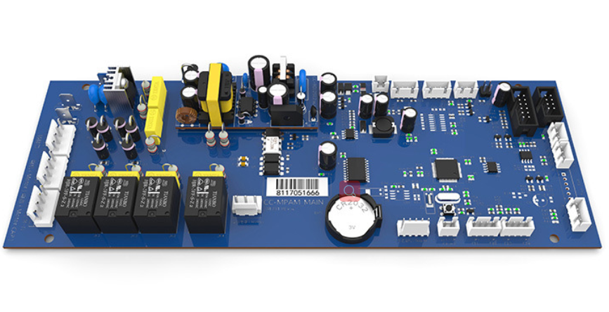
In the design and manufacturing process of electronic equipment, printed circuit design is one of the core links. First, it is necessary to conduct circuit schematic design to clarify the connection relationships and functional logic of electronic components. Then, it proceeds to PCB layout design; considering requirements such as electromagnetic compatibility (EMC) and heat dissipation, the arrangement of components and the routing of wires are reasonably planned.
After the design is completed, the scheme is verified and optimized through simulation. Subsequently, production files are generated and transmitted to the manufacturing stage, which connects with subsequent steps such as substrate processing and component assembly, forming a complete closed loop from design to finished product.
2.Applied Materials for Printed Circuit Boards
Applied materials for printed circuit boards are crucial to their performance. Commonly used substrate materials are glass fiber reinforced epoxy resin boards, which offer excellent insulation properties and mechanical strength. Conductive layers primarily use electrolytic copper foil, with thickness selected based on current carrying requirements to ensure stable signal transmission. Solder mask materials are mostly photosensitive inks, which protect copper foil from oxidation and external damage while facilitating subsequent assembly. Silk screen inks, on the other hand, are used to mark component numbers and parameters, making maintenance and identification easier.
3.Characteristics of Printed Circuit Board Manufacturing Process
The manufacturing process of printed circuit boards (PCBs) features high precision and automation. From substrate cutting and CNC drilling to chemical copper plating and pattern electroplating. And then to etching forming and solder mask coating, each process requires strict precision control. For example, the error of drilling hole diameter is usually controlled within ±0.05mm. With the development of technology, the application of equipment such as laser direct imaging (LDI) and automated electroplating lines has further improved production efficiency and product consistency. It meets the needs of miniaturization and high density of electronic devices.
4.Printed Circuit Board Assembly Technology
Printed Circuit Board (PCB) Assembly Technology mainly includes Surface Mount Technology (SMT) and Through-Hole Technology (THT). SMT has the advantages of high assembly density and small size, and is suitable for surface mount components. Its assembly is completed through three processes: solder paste printing, component placement, and reflow soldering. THT, on the other hand, is suitable for components with more pins or higher power, and adopts the processes of component insertion and wave soldering.In actual production, these two technologies are often combined to ensure the complete functionality and reliability of the circuit board, and to meet the assembly needs of different types of electronic equipment.