Printed Circuit Board Design, which is the first step to change your concept into a real PCB. This job seems to be a complex work and needs more patience and more experienced engineers to finish it. In gereral, there seems to have 11 steps for the PCB designers to reference when they are ready to design.
Step 1: Finalize Your Printed Circuit Board Design:
Everything starts with the circuit layout, and without which, there may be no need for a pcb. During the antique days, people usually hand draw maximum circuits and later capture them electronically. In these days’s international of current computing, the circuit design is capture without delay into a schematic. But for the sake of readability we’ve added this as step 1 inside the pcb layout guide.
Step 2: Choose PCB Layout Software
Regularly electric engineers don’t have a desire in terms of deciding on the pcb design software program. Their corporations have invested lots into software applications and all their legacy layout are captures in those applications, and consequently are “stuck”. However the hobbiest has numerous alternatives. It’s important to choose a bundle that is first and important clean to apply. However, also able to finishing the pcb design as a few programs gained’t be capable of handle the complexity.
Step 3: Capture Your Schematic
As noted earlier, its probably that the designer captured the circuit design electronically from the start. In popular “shooting the schematic” is the process. And via which every component is drawn electronically and are interconnected with each other.
Step 4: Design Factor Footprints
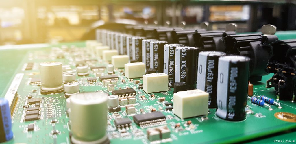
As soon as the schematic finished, it’s time to attract the bodily outline of each of the additives. We finally need to place these outlines onto the copper foil and to solder components onto the broadcast wiring board.
Step 5: Set-up PCB Define
Every task could have restrictions associated with the board define. We should determine it on this step. Because we need to have an concept of factor depend and the area recognised.
Step 6: Setup Layout Regulations
With the pcb outline and pcb footprints completed, it is time to start the location. But before placement notion, you must setup the design rules. So that we can make sure that components or lines aren’t too close to each other. That is only one example. And there may have loads of various rules that we can use to implement a pcb layout.
Step 7: Location Additives
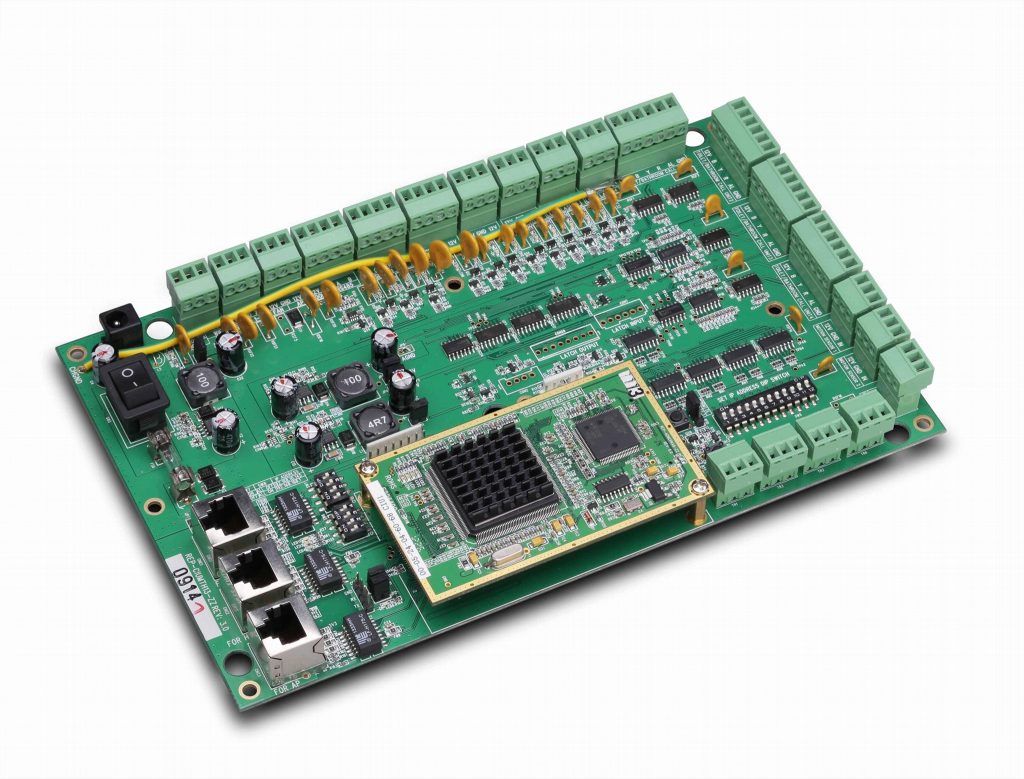
Its time to transport each component onto the pcb and start the tedious paintings of creating all those components match collectively. that is wherein you’ll discover that pcb design is actually a jigsaw puzzle.
Step 8: Manual Route Strains
It’s necessary to manually path vital strains. clocks. electricity. sensitive analog strains. Once that’s entire you can flip it over to step nine.
Step 9: The Usage of The Automobile Router
There are a handful of rules to be able to carry out for the usage of an autorouter. However doing so will save you hours if not days of routing lines.
Step 10: Run Design Rule Checker
Most pcb layout software applications have a superb setup of design rule checkers. It’s clean to violate PCB spacing policies. This will pinpoint the error saving you from having to respin the pcb.
Step 11: Output The Gerber Documents
Once the board is errors loose, it’s time to output the gerber documents. The pcb fabrication service providers usually need thes files to fabricate your published circuit board.
Editor: Kevin Tian, Contact me: [email protected]