PCB Trace Material is a conductive path. It carries signals between components. These copper pathways form circuits. Essentially, they replace traditional wires. Their design affects circuit performance. Proper width is crucial for current.
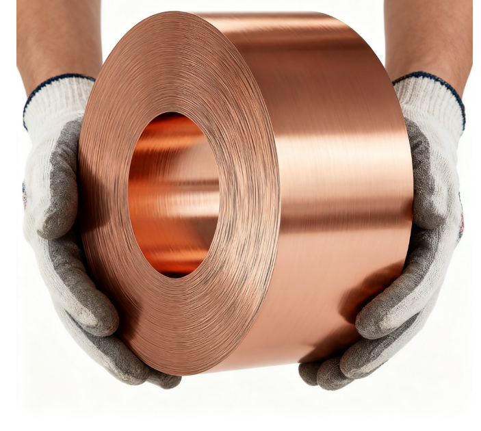
1.Copper’s Superior Properties PCB Trace Material
Copper offers excellent electrical conductivity. This ensures minimal signal loss. It also provides great thermal conductivity. Heat dissipates efficiently from traces. Furthermore, copper is highly ductile. It withstands manufacturing processes well. Moreover, it’s readily available. This makes it cost-effective.
2. Designing Optimal Traces PCB Trace Material
First calculate required trace width. Consider current carrying capacity. Account for temperature rise too. Maintain consistent impedance for high frequencies. Avoid sharp 90-degree angles. Use curved corners instead. This prevents signal reflections. Also keep traces short.
3. Manufacturing Process Overview
Start with copper-clad laminate. Apply photoresist layer first. Then expose it to UV light. Develop to remove unexposed areas. Etch away unwanted copper. Finally strip remaining photoresist. This forms precise trace patterns.
4.Why Choose Copper
Compared to aluminum, copper conducts better. It has higher melting point too. Silver might conduct slightly better. But copper is more affordable. Gold offers good corrosion resistance. However copper is more practical. Thus copper remains optimal.

5.Quality Verification
Always perform electrical testing. Check for open and short circuits. Measure trace resistance values. Verify impedance matching too. Use automated optical inspection. This ensures manufacturing quality. Finally test thermal performance.
In summary, traces form circuit connections. Copper provides ideal characteristics. Its conductivity balances cost perfectly. Proper design ensures reliability. Careful manufacturing guarantees performance. Therefore copper remains dominant.
Future Material Developments
New materials are being researched actively. Graphene shows promising conductivity potential. It might surpass copper’s performance. However, production costs remain high. Silver alloys also offer alternatives. Yet copper maintains cost advantages. Carbon nanotubes present new possibilities. But stability challenges persist.
Practical Design Considerations
Always consult manufacturer’s capabilities. They provide design guidelines clearly. Consider environmental factors carefully. Humidity affects copper oxidation rate. Use solder mask protection wisely. It prevents accidental short circuits. Implement teardrops at pad connections. This strengthens mechanical reliability.