PCB Industry will be advantage on 5G communication, this is the common sense now. The PCB industry will power the 5G revolution. 5G is a very hot topic in the PCB industry, and 5G communication has high-frequency, high-speed, high-performance, low-latency and high-capacity characteristics. This will bring terminal intelligence, network efficiency, information data and everything.
The arrival of the 5G era will drive a series of related industries to upgrade. Eespecially in the fields of 5G communication, IoT, automotive electronics, big data, industrial interconnection and AI. As old saying, PCB is the mother of electronic products. It is estimated this will really bring the more largest opportunities for printed circuit baords. And the PCB industry will enter a new round of production cycle.
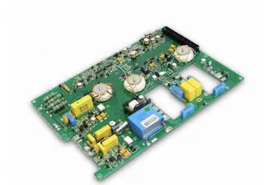
The transformative potential of 5G technology—promising blazing speeds, ultra-low latency, and massive device connectivity—relies on a complex ecosystem of advanced hardware. At the heart of this ecosystem, the Printed Circuit Board (PCB) industry plays a foundational and critical role, acting as a key enabler for the 5G revolution.
The leap to 5G’s high-frequency bands, including millimeter-wave (mmWave), presented a monumental challenge. At these frequencies, signal loss and integrity become paramount. Traditional PCB substrates like FR-4 were insufficient, necessitating a industry-wide shift towards high-performance materials. Advanced laminates with stable dielectric constants (Dk) and extremely low dissipation factors (Df), became essential. These specialized materials minimize signal attenuation and phase distortion, ensuring that high-frequency 5G signals are transmitted with minimal loss and maximum integrity across devices and infrastructure.
Furthermore, sophisticated PCB design make the implementation of massive Multiple-Input, Multiple-Output (MIMO) antenna technology, a cornerstone of 5G possible. Base station antennas now contain hundreds of antenna elements, all integrated onto a single PCB. This demands advanced High-Density Interconnect (HDI) processes. This allows for finer lines, micro-vias, and multiple layers within an incredibly compact form factor. The density and precision of these boards are a direct result of PCB manufacturing innovations.
Thermal management is another critical area where the PCB industry rises to the challenge. 5G’s increased power and processing generate significant heat. To maintain reliability and performance, we are engineering PCBs with enhanced thermal dissipation properties. This includes the use of heavy copper coils, insulated metal substrates (IMS). And sophisticated thermal vias to effectively draw heat away from powerful RF components and processors.
From the intricate motherboards inside 5G smartphones to the active antenna units (AAUs) on macro and small cell towers. And the high-speed servers in data centers, advanced PCBs are the unsung heroes. They provide the essential platform that interconnects chips, antennas, and components. Determining the ultimate performance, efficiency, and reliability of the entire network.
In conclusion, the 5G era is not just driven by software and protocols, but also is fundamentally built on hardware innovation. The PCB industry, through its advancements in materials science, precision manufacturing, and thermal design, has provided the essential physical foundation for 5G. It is this silent enabler, constantly evolving to meet extreme technical demands, that is truly powering the connected future.