PCB laser marking is required more and more with the development of goods tracing ability in current economy.

The basic principle of PCB laser marking is that a high-energy continuous laser beam is generated by a laser generator. The focused laser acts on the printing material, which instantly melts or even vaporizes the surface material. By controlling the path of the laser on the surface of the material, The required graphic marks are formed. Both the fiber laser and the CO2 laser use the thermal effect of the laser on the material to achieve the marking effect. Basically, the surface layer of the material is destroyed to form a rejection effect, which leaks out the background color and forms the color difference. The green laser uses the chemical reaction of the laser to the material to cause the color of the material to change, and then does not produce a rejection effect, forming graphics and characters without obvious touch.
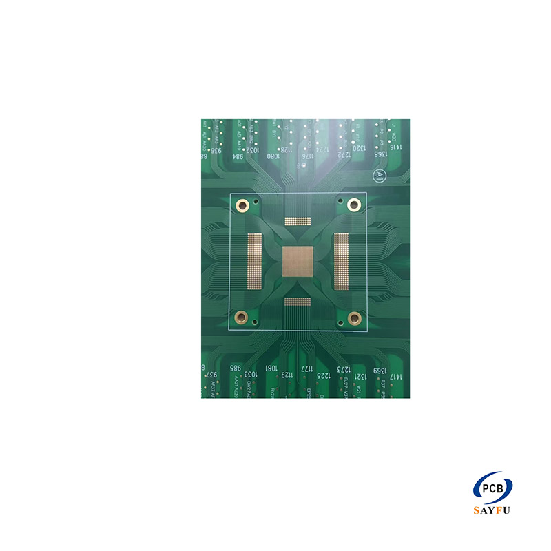
PCB laser marking technology is one of the largest application areas of laser processing. Laser marking is a method that uses a high-energy-density laser to locally irradiate a workpiece to vaporize the surface material or change the color of the chemical reaction, leaving a permanent mark. Laser marking can produce a variety of characters, symbols and patterns, and the character size can be on the order of millimeters to micrometers, which has special significance for the anti-counterfeiting of PCB products.
QR Code: one Implementation of PCB Laser Marking (2025 Update)
The integration of QR codes onto printed circuit boards (PCBs) involves a precise laser etching or silkscreen printing process:
Design Phase: The QR code (containing traceability data, version control, or part numbers) is embedded into the PCB design file (e.g., Gerber), ensuring sufficient contrast and size (minimum 10×10mm for readability).
Fabrication:
Laser Marking: High-precision lasers etch the code onto solder masks or copper layers, ideal for harsh environments.
Silkscreen Printing: UV-resistant ink prints the code on the PCB surface, cost-effective for high-volume production.
Verification: Automated optical inspection (AOI) validates readability post-fabrication.
Applications: Inventory tracking, counterfeit prevention, and IoT device authentication. Advances in miniature QR codes (e.g., 5×5mm) now support denser data storage.