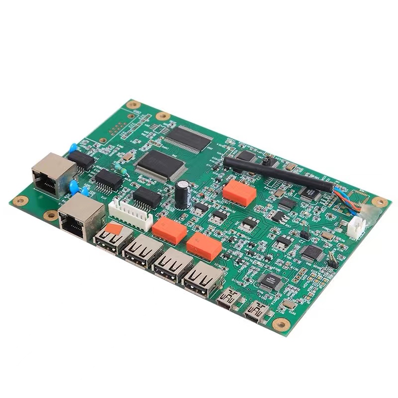
PCB for optoelectronic devices industry is a new theme for modern electronics with the development of modern technology. The optoelectronic devices industry, encompassing technologies like LEDs, laser diodes, photodetectors, and image sensors, is a cornerstone of modern innovation, driving advancements in telecommunications, healthcare, and consumer electronics. At the heart of these sophisticated systems lies a critical, yet often overlooked, component: the printed circuit board (PCB). The unique demands of optoelectronic applications have propelled the evolution of PCBs from simple electrical interconnects into highly specialized platforms that are fundamental to performance and reliability.
Unlike standard electronic PCBs, those for optoelectronics must manage a complex interplay of electrical, optical, and thermal energy. This necessitates specialized materials and designs. Standard FR-4 substrates are often inadequate due to their higher electrical loss and poor thermal performance at high frequencies. Instead, high-frequency laminates like Rogers, PTFE (Teflon), or ceramic-filled materials are preferred. These substrates provide stable dielectric constants and low loss tangents. Which are crucial for maintaining signal integrity in high-speed data transmission, such as in fiber optic transceivers.
Thermal management is arguably the most critical challenge. High-power LEDs and laser diodes generate significant heat, which can degrade performance, shift optical wavelength, and drastically shorten lifespan. Optoelectronic PCBs address this through metal-core PCBs (MCPCBs), particularly those with aluminum cores. These boards feature a thermally conductive dielectric layer that efficiently transfers heat from the components to the metal substrate. Which acts as a heat sink. For the most demanding applications, insulated metal substrates (IMS) are used to provide even superior thermal dissipation.
Furthermore, the design and layout of these PCBs are paramount. Precise impedance control is necessary for high-speed electrical signals driving lasers or coming from photodetectors. The physical placement of optical components must be exact to ensure proper alignment with waveguides, lenses, or optical fibers integrated onto or above the board. This often involves sophisticated techniques like creating cavities or using transparent substrates for back-side emission or detection.
In conclusion, as optoelectronic devices become faster, smaller, and more powerful. The PCB is no longer just a passive carrier but an active enabler. The continued development of advanced PCB materials, thermal management strategies. And integration techniques is essential for pushing the boundaries of what is possible in the dynamic and rapidly growing optoelectronics industry.
