A Printed Circuit Board is fundamental. It is in almost every electronic device. Understanding a PCB Components & Trace is a key skill. It helps with debugging and repair. It also aids in design. This guide will teach you how. We will focus on components and traces.
1.Identifying Common PCB Components
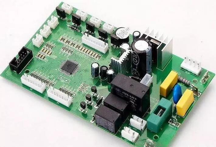
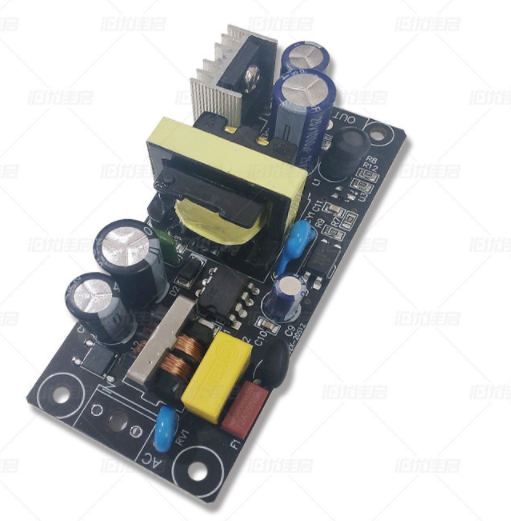
First, look at the board‘s components. These are the electrical parts. They define the board’s function. Start with large integrated circuits. These are often the brains. They are called chips or microcontrollers. They have many connecting pins.
Then, find resistors on the board. They control the flow of current. They usually have colored stripes. These are color codes. They indicate the resistor’s value. Capacitors are also common. They store and release energy. They look like small cylinders or blocks.
Do not forget diodes and LEDs. Diodes allow current one way. LEDs are a type of diode. They emit light when active. Transistors are amplifiers or switches. They have three connecting legs. Look for large connectors too. These bring power or signals.
Also, identify the inductors and crystals. Inductors store energy in a magnetic field. Crystals provide a precise clock signal. They look like metal cans. Each component has a symbol. This is printed on the silkscreen.
2.Understanding Traces and Connections
Now, observe the copper traces. These are the board’s wiring. They connect all the components. Traces are thin lines. They are made of copper. They carry electrical signals.
Look closely at the board’s surface. You will see a network. This is the trace layout. Traces can be on top. They can also be on the bottom. Many boards have multiple layers. So traces can be inside.
Vias are very important too. They are small holes. They connect traces between layers. Think of them as tunnels. Pads are where you solder. Components connect to pads. Pads connect to traces.
The ground plane is a large area. Power traces are often wider. They carry more current. This prevents overheating.
3.Practical Steps for Reading a PCB Components & Trace
Gather your tools first. You need good lighting. A magnifying glass helps. A multimeter is essential. It tests connections and values.
Start with the schematic diagram. This is the circuit’s map. It shows logical connections. Compare it to the physical board. Find the main components first. Then follow the signal path.
Use the silkscreen layer for help. It has letters and numbers. “R” means resistor. “C” means capacitor. “U” is for integrated circuits. This labeling is very useful.
Check for power and ground. Find the power input connector. Trace its path on the board. See where it goes. Locate the ground plane. It is usually easy to find.
Use your multimeter for testing. Set it to continuity mode. This checks for connections. Touch two points with probes. A beep means they are connected. This finds broken traces.
Look at the solder joints too. They should be shiny and smooth. Bad joints are dull or cracked. They can cause failures. Re-solder them if needed.
Practice is the best teacher. Start with simple boards. Then move to complex ones. Soon reading a PCB will be easy. You will see the story it tells.