PCB assembly design rules are the cornerstone of reliable, manufacturable high-performance PCBs. These guidelines serve as a bridge between design intent and production reality. This connection directly influences assembly yield and signal integrity.
PCB Stackup Design: Balancing Electrical Performance and Manufacturability
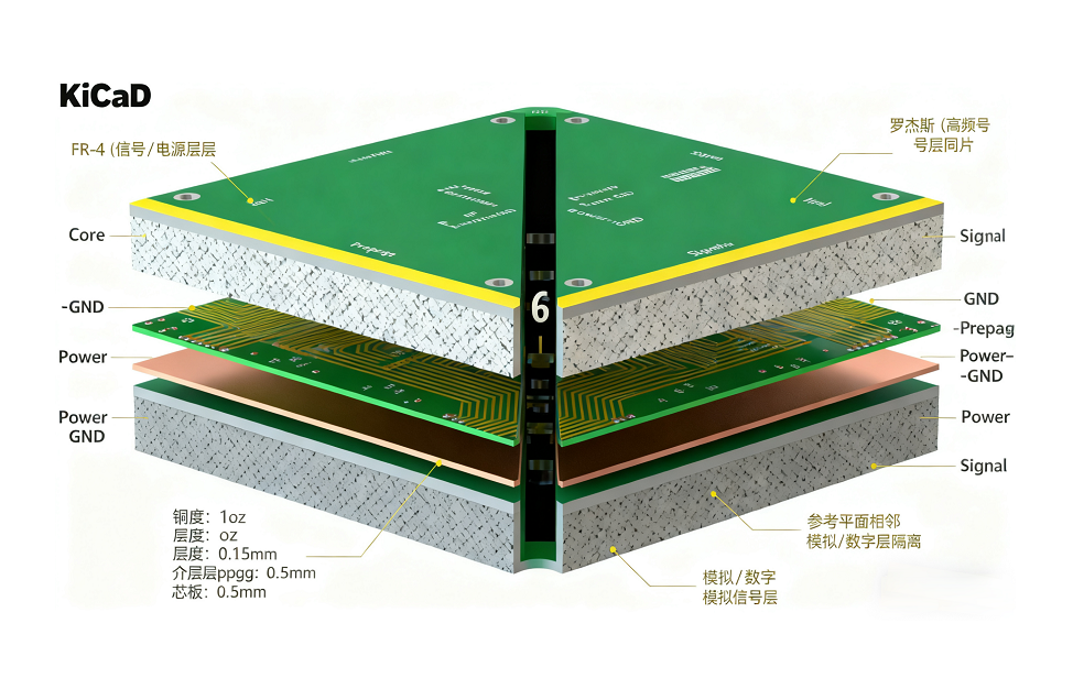
A key part of these rules is PCB stackup design. Rational stackup planning balances electrical performance and manufacturability. Designers define layer counts by signal density: high-frequency designs need dedicated ground/power planes to reduce noise, while HDI PCBs require thin dielectrics for fine-pitch components. Material selection matters too—low-loss dielectrics (e.g., Rogers) suit high-speed signals, while power boards need thermally conductive materials. Stackup rules also mandate signal layers adjacent to reference planes for impedance control and isolate analog/digital layers to minimize crosstalk. Tools like Sayfu Designer simplify this with pre-built templates and real-time calculations.
Pad and Footprint Matching Rules: Getting the Fit Right
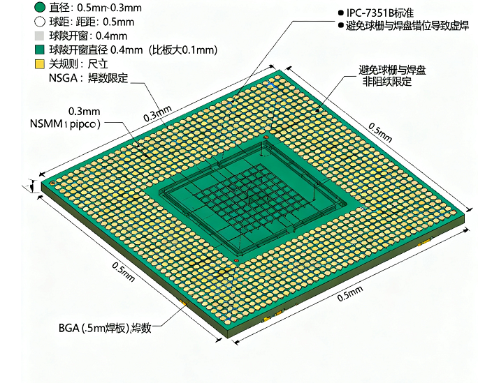
Matching PCB pads with component footprints is key for reliable assembly. These rules make sure pad size, spacing, and shape line up with a component’s leads or terminals—whether it’s a small SMT part, a BGA, or a through-hole component. For example, if an SMT pad is too big or too small, solder might either connect adjacent pads (causing shorts) or not stick well (weakening the joint). For BGAs, the pad grid must match the component’s ball grid exactly to avoid bad connections when soldering. Also, pad designs need enough space around them (clear of solder mask) to make sure solder paste goes on evenly—this helps keep both the physical and electrical connections strong.
Other Core Assembly Design Rules
Other core rules include component placement (avoiding connector overcrowding), pad design (meeting IPC standards for solder joint strength), and thermal management (placing heat-generating parts near heat sinks). Conductor clearance prevents short circuits, and solder mask specs ensure proper reflow. Adhering to these rules,especially stackup best practices—cuts rework and costs, guaranteeing PCBs perform as intended in real-world use.