The application of multilayer FPC boards
Multilayer FPC boards are vital for modern electronics. They fit complex wiring into tiny spaces. You find them in compact smartphones and wearables. They are also used in reliable automotive systems. These circuits enable advanced medical devices too. Essentially, they drive innovation across industries.
Summarized Workflow for multilayer FPC boards :
Material Preparation
The selection of materials for multilayer FPC boards is of great importance.And the process begins with selecting a flexible substrate, typically polyimide or polyester, due to its heat resistance and mechanical durability.Manufacturers laminate copper foil onto the substrate using adhesives or adhesiveless methods (e.g., sputtering). For multilayer designs, inner layers are pre-etched with circuit patterns via photolithography: photoresist is applied, exposed to UV light through a mask, and chemically etched to remove unwanted copper.
Layer Stacking and Lamination
Multiple layers PI are aligned and bonded under high temperature (170–200°C) and pressure (200–400 psi) using prepreg (B-stage resin) as an adhesive. Critical steps include “black oxidation” or “browning” of inner copper layers to enhance adhesion and prevent delamination.
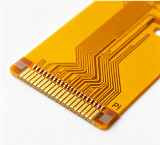
PTH and Outer Layer Processing for multilayer FPC boards
Drill microvias and through-holes mechanically or with lasers, and then plate them with copper to establish interlayer connections. Advanced techniques like laser drilling ensure precision for high-density designs.
Pattern and etch the outer circuits, similar to the inner layers. Then, laminate a protective coverlay (a polyimide film) or solder mask to insulate the traces, ensuring openings remain for the solder pads. If needed, add stiffeners (e.g. FR4,PI,Steel) to reinforce specific areas.
Testing and Finishing
Electrical tests verify continuity, followed by surface finishing (e.g., ENIG) to prevent oxidation. Final inspection ensures quality before singulation.This streamlined process balances flexibility and complexity, enabling compact, high-performance multilayer flexible printed circuit boards.
Packaging
FPC packaging refers to the final assembly and protection of multilayer FPC boards . This process involves critical steps like applying coverlays or solder masks. These layers insulate the circuits and expose solder pads. Stiffeners are also added for structural support in specific areas. Effective packaging ensures the FPC’s reliability in the end product.