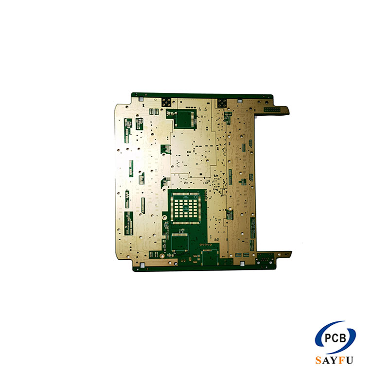
Multilayer circuit boards Design: Impact of Copper Weight, Trace Width/Spacing on Electrical Performance
Multilayer circuit boards enables high-density interconnections in modern electronics, where copper thickness (weight), trace width, and spacing critically influence electrical performance.
Here’s a structured analysis:
Design Tradeoffs & Trends Performance vs. Cost:
Thick copper (≥3 oz) and ultra-fine traces (<2 mil) boost performance but escalate manufacturing complexity and cost.
High-Frequency/HPC Focus:
Modern designs prioritize impedance-matched traces (e.g., 50Ω single-ended, 90Ω differential) and low-loss materials to mitigate signal degradation.
Conclusion
Optimizing copper weight, trace width, and spacing requires balancing electrical needs (current, speed, noise) with manufacturability. As multilayer circuit boards trend toward higher density and thinner features, simulation tools and standardized design rules (e.g., IPC-2152) become indispensable .
Copper Thickness (Weight)
Current-Carrying Capacity:
Thicker copper (e.g., 2 oz vs. 1 oz) increases cross-sectional area, reducing resistance (R ∝ 1/cross-section) and enabling higher current flow without overheating. For example, 2 oz copper handles ~1.5× more current than 1 oz at identical widths.
Thermal Management:
Enhanced thermal conductivity dissipates heat efficiently, preventing hotspots in high-power circuits (e.g., power supplies).
Signal Integrity:
Thicker copper reduces resistive losses and skin effect, minimizing signal attenuation in high-frequency/RF applications.
Trace Width
Current Density & Heat:
Wider traces lower current density (J = I/A), reducing Joule heating. A rule of thumb: 0.15 × Width (mm) ≈ Max Current (A) for 1 oz copper.
Impedance Control:
Critical for high-speed signals (e.g., DDR, PCIe) in multilayer circuit boards. Narrower traces increase resistance (R ∝ 1/width), affecting characteristic impedance (Z₀). Designers use formulas like 0.0005 × L/W (length/width) to optimize.
Space Efficiency:
Miniaturization demands narrower traces but risks exceeding fab capabilities (e.g., < 3.5 mil width requires advanced processes) .
Trace Spacing
Crosstalk Prevention:
Insufficient spacing increases capacitive coupling, causing noise in adjacent traces. For ≥100V signals, spacing ≥8 mil is typical to avoid arcing.
Manufacturing Limits:
Standard processes support 6/6 mil (width/spacing), while <3.5/3.5 mil raises costs and defect risks .
Guangdong Sayfu Multilayer Circuits Co.,Ltd is focus on high density multilayer boards, if any question on the design phase, please contact with us.