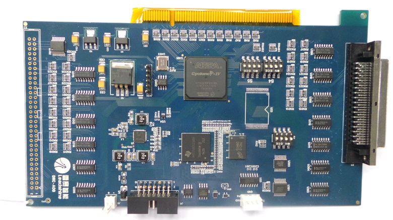
Mixed-Signal IC Design and verification is an important topic or theme for modern electronics development. The modern semiconductor landscape is dominated by Systems-on-Chip (SoCs) that seamlessly bridge the digital and physical worlds. At the heart of these powerful chips lies mixed-signal integrated circuit (IC) design. A discipline dedicated to creating circuits that process both continuous analog signals and discrete digital data on the same silicon die. From smartphones connecting to wireless networks to sensors interpreting real-world phenomena like temperature and sound, mixed-signal ICs are the indispensable translators of our digital age.
The design process is a complex, hierarchical endeavor. It begins with top-level architectural definition, partitioning system functions into analog and digital blocks. Analog designers craft sensitive circuits like amplifiers, oscillators, and data converters (ADCs/DACs). Which must be robust against noise, process variations, and non-ideal effects. Digital designers, meanwhile, implement logic and signal processing functions using automated tools for synthesis and place-and-route. The paramount challenge is ensuring harmonious coexistence. The fast-switching digital circuits can generate significant noise that corrupts delicate analog signals through the shared substrate and power supply lines. Careful floorplanning, isolation techniques, and the use of guard rings are critical to mitigate these issues.
Given this inherent complexity, verification is arguably as crucial as the design itself. Mixed-signal verification employs a multi-faceted approach. A cornerstone technique is the use of analog behavioral models in a digital simulation environment. These models, written in languages like Verilog-AMS or SystemVerilog, abstract the analog block’s functionality. And allowing for fast, system-level simulations that would be prohibitively slow using full transistor-level SPICE simulations. This co-simulation enables early validation of interactions between the digital control logic and the analog front-end.
However, behavioral model simulation is not sufficient. Transistor-level post-layout simulation is an essential final step. After the physical layout is complete, extracted parasitics (resistances and capacitances) are back-annotated into the circuit netlist. Running SPICE simulations with these real layout effects confirms that the circuit still meets its performance specifications under realistic conditions, checking for critical issues like timing, stability, and signal integrity.
In conclusion, mixed-signal IC design and verification is a delicate art of balancing two contrasting engineering domains. It demands deep, specialized knowledge in both analog and digital disciplines, coupled with a rigorous and layered verification methodology. As the demand for more intelligent, connected, and efficient electronics grows, the role of robust mixed-signal design will only become more central to advancing semiconductor technology.
