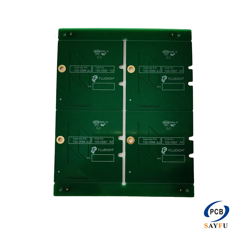
An IC Substrate manufacturer is a highly sophisticated printed circuit board (PCB) that serves as the critical interface between a delicate semiconductor chip and a main PCB, like a motherboard. Think of it as an intelligent translator and a sturdy bridge. It provides the electrical connection from the chip’s incredibly fine-pitched pins to the coarser traces of the board. Furthermore, it efficiently dissipates heat and provides crucial mechanical support and protection for the fragile silicon die, which is often only a few millimeters in size.
Pushing the Limits of Miniaturization for IC Substrate manufacturer
IC substrates represent the pinnacle of PCB manufacturing technology. They are High-Density Interconnect (HDI) products pushed to the extreme. Features like micro-vias, ultra-fine line widths and spacings, and complex multi-layer builds (often exceeding 10 layers) are standard. The most advanced type is the Flip-Chip (FC) BGA substrate, where the chip is mounted directly upside-down onto the substrate. This demands exceptional flatness and precision to ensure all connections are perfect, enabling the high-speed performance required by modern processors.
Enabling the Modern Electronics Era
Without the constant innovation in IC substrate technology, the advancement of powerful, compact electronics would be impossible. They are the unsung heroes inside every device that relies on cutting-edge chips. You will find them in smartphones, laptops, AI accelerators, and high-performance servers. As chips continue to get faster, smaller, and more powerful, the demands on IC substrates to handle higher signal speeds, greater power density, and improved thermal management will only intensify, ensuring their role as a vital enabler of future technology.
The future lies in even finer features and the integration of passive components directly within the substrate itself. This “embedding” technology promises greater miniaturization, enhanced electrical performance, and improved reliability for next-generation chips, pushing the boundaries of what’s possible in electronics packaging.
If you need to know about PCB news ,please pay attention http://www.sfmpcb.com/ .
