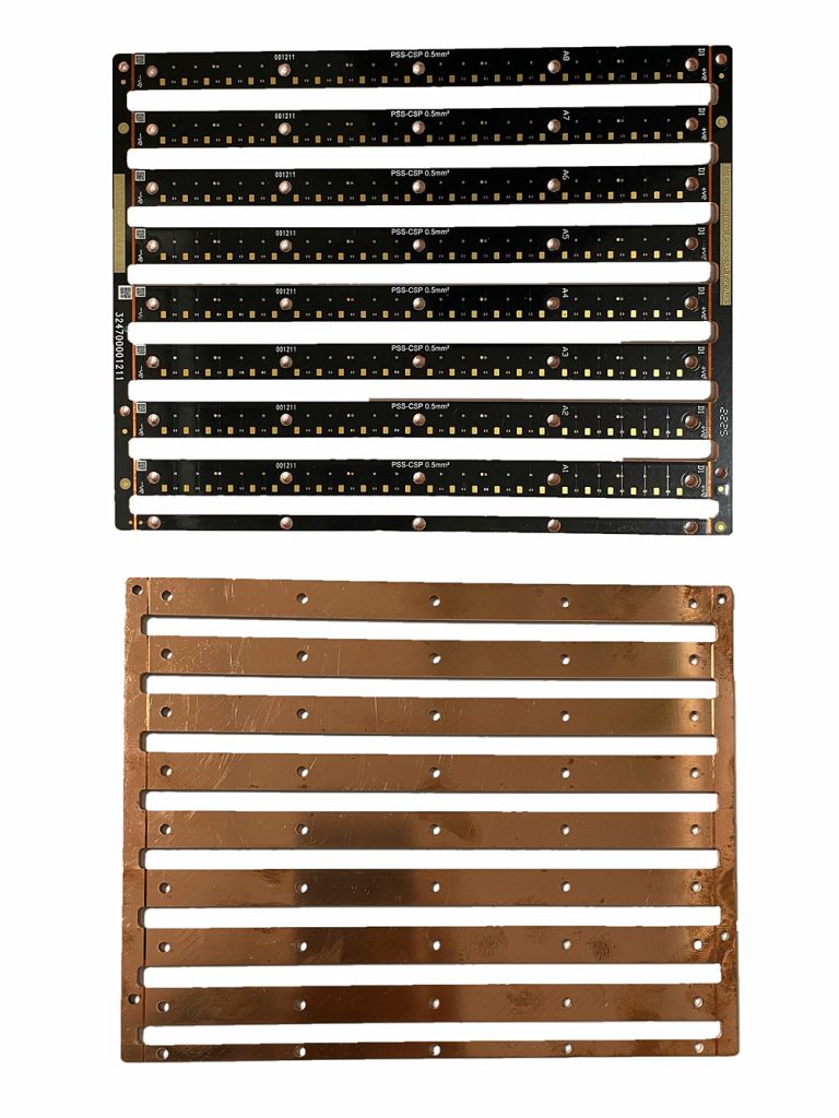
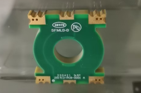
In High-Speed PCB Design, signal integrity has evolved from a specialized skill into a critical factor determining product success. It focuses on the ability of a signal to travel through PCB transmission paths without waveform distortion. As clock frequencies climb to hundreds of megabits or even gigabits per second, the interconnects on circuit boards are no longer mere electrical connections but exhibit complex transmission line effects. Any oversight in design can lead to sharp declines in system performance or even functional failure.
1.Controlling Impedance Discontinuities for High-Speed PCB Design
The key to ensuring signal integrity lies in controlling reflections and losses. Impedance discontinuities are the primary cause of reflections. When inconsistencies such as sudden changes in trace width, vias, connectors, or improper topology occur along the signal path, part of the signal energy reflects back to the source. This results in overshoot, undershoot, or even logical errors at the receiving end. The solution lies in implementing strict impedance control, which involves precisely calculating and maintaining consistent characteristic impedance (e.g., 50Ω for single-ended, 100Ω for differential) based on the layer stack-up and dielectric materials.
2.Managing Transmission Losses for High-Speed PCB Design
Transmission losses cannot be ignored at higher speeds. Conductor loss (due to skin effect) and dielectric loss (related to the loss tangent) intensify with increasing frequency, leading to smoothed signal edges and reduced amplitude. To address this challenge, designers must carefully select low-loss laminate materials and use simulation tools to pre-analyze channel performance. Techniques such as pre-emphasis or equalization may be employed to compensate for losses when necessary.
3. Optimizing PCB Stack-up Configuration
Proper stack-up design is crucial for maintaining signal integrity in multi-layer boards. The arrangement of signal, power, and ground layers directly affects impedance control and electromagnetic compatibility. A well-designed stack-up provides adequate shielding, minimizes crosstalk, and ensures stable reference planes. Designers must consider factors like layer sequencing, dielectric thickness, and material properties to achieve optimal performance while controlling manufacturing costs.
4.Implementing Effective Termination Strategies
Appropriate termination techniques are essential for minimizing signal reflections at both source and receiver ends. Different termination methods – such as series, parallel, and Thevenin termination – serve specific application scenarios. The choice of termination strategy depends on factors like signal frequency, drive capability, and power consumption requirements. Proper termination not only reduces ringing and overshoot but also improves signal quality at the cost of minimal additional power consumption.

5.Addressing Crosstalk and EMI Concerns
As PCB layouts become more dense, crosstalk between adjacent signals and electromagnetic interference emerge as critical challenges. Crosstalk occurs through capacitive and inductive coupling between parallel traces, potentially causing false triggering and timing errors. Implementing guard traces, maintaining sufficient spacing, and using differential signaling are effective countermeasures. Simultaneously, proper grounding and shielding techniques help meet electromagnetic compatibility requirements while reducing radiated emissions.
In summary, ensuring signal integrity in high-speed designs is a systematic endeavor. It requires designers to deeply understand transmission line theory and to employ precise impedance control, rational material selection, comprehensive return path planning, and forward-looking simulation analysis. Together, these practices safeguard the stable and clean “pulse” of digital systems, laying a solid foundation for product reliability.
