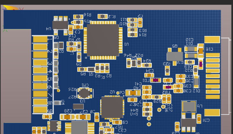
High-frequency PCB design refers to the process of designing a circuit board that can precisely transmit high-frequency signals. Before conducting high-frequency PCB design, it is necessary to understand what high-frequency means and some of the design rules for high-frequency PCBs. Adhering to these design rules can ensure that signals are not disturbed. High-frequency refers to frequencies typically above 1GHz. For such designs, conventional techniques cannot meet the requirements for signal integrity and performance. At these frequencies, interfering signals may cause problems such as signal attenuation, crosstalk, and electromagnetic interference (EMI).
How to Design High frequency PCB
When conducting high-frequency PCB design, several core principles must be followed. The first is material selection. Common FR-4 material has high loss at high frequencies, so specialized high-frequency boards such as Rogers and Taconic should be used. These materials have stable and low dielectric constants (Dk) and loss factors (Df). Secondly, strict impedance control is necessary. The target characteristic impedance (such as 50Ω or 100Ω differential) is achieved through precise calculation of trace width, dielectric thickness, and dielectric constant, while maintaining consistency throughout the trace path. Thirdly, the wiring strategy should be optimized. Critical signal lines should be as short and straight as possible, avoiding sharp 90-degree corners. Use 45-degree or arc-shaped corners to reduce signal reflection. At the same time, providing a continuous and closely spaced reference ground plane for each high-frequency signal line is the basis for controlling the return path and reducing radiation noise.
Signal integrity and shielding measures
Ensuring signal integrity is a high-level requirement. This involves reducing crosstalk by increasing the spacing between parallel traces or inserting ground lines for isolation. Via design is also crucial and should be minimized as each via introduces parasitic inductance and impedance discontinuity. Back-drilling techniques can be used to remove the remnants of via holes when necessary. For strong interference sources or sensitive circuits, shielding measures are required, such as using shielding covers or ground copper foil to isolate the analog/digital sections and the RF unit. Finally, using electromagnetic simulation software for SI/PI analysis after layout can help identify potential issues in advance, significantly increasing design success rates and reducing prototyping costs.
