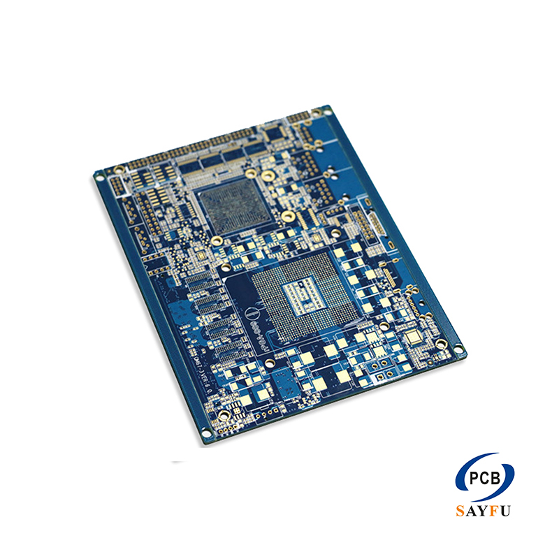
Manufacturing Process of High-Density Interconnection (HDI) PCBs
High Density Interconnection PCB are characterized by their fine lines, micro-vias (blind/buried vias ≤ 0.10mm in diameter), and high wiring density (≥600 vias/in²), enabling compact, high-performance electronics.
The core process involves:
Material Selection & Layup:
Specialized materials like Resin Coated Copper (RCC) (e.g., 65T/100T types) or thin laminates are used to achieve the required thin dielectric layers for laser drilling. The stack-up structure (e.g., 1+C+1, 2+C+2) is meticulously planned to optimize functionality while minimizing production steps like lamination.
Laser Drilling (Micro-Via Formation):
Laser drilling (e.g., UV or CO₂ lasers) replaces mechanical drilling to create micro-vias (typically 0.10mm or smaller) in High Density Interconnection PCB. Precise alignment using LDI (Laser Direct Imaging) fiducial marks is critical. Parameters are adjusted based on RCC thickness (≤55µm for 4mil vias, ≤100µm for 5mil) to ensure clean via walls and avoid resin ablation defects. Test coupons are drilled and cross-sectioned first for quality verification.
Lamination:
Multiple sequential lamination cycles under specialized pressure and temperature profiles bond the layers together. For PCBS with buried vias, pre-treatment baking (e.g., 110°C for 1 hour) after browning is essential. Post-lamination dimensional stability (shrinkage/expansion) is measured to adjust subsequent drilling files.
Via Metallization & Plating:
Micro-vias undergo desmearing (gentle mechanical brushing and high-pressure water wash with vias facing down) and electroless copper deposition (chemical copper) to make them conductive. Electroplating then builds up copper thickness within the vias and on traces. Strict parameters (e.g., 12 ASF * 10min + 5 ASF * 170min for panel plating) ensure minimum copper thickness requirements (avg. ≥18µm for first article, ≥15µm for production) are met.
Patterning & Etching:
Laser Direct Imaging (LDI) exposes ultra-fine line photoresist patterns (≤0.10mm width/spacing) with high precision. Chemical etching removes unwanted copper, forming the intricate circuitry.
Inspection & Testing:
Rigorous cross-sectioning validates via copper thickness and structure integrity. Automated Optical Inspection (AOI) checks for defects. Advanced fixtures enable high-throughput testing of multiple coupons simultaneously.
This optimized process achieves the high density, reliability, and miniaturization demanded by modern electronics like smartphones and wearables.
Practical Applications of High Density Interconnection PCB
High Density Interconnection PCB are essential enablers for modern, compact, and high-performance electronics. Their core advantages of finer lines/spaces, micro-vias (including blind and buried types), and significantly increased wiring density translate into critical real-world applications:
Miniaturized Consumer Electronics:
HDI technology is fundamental to the shrinking size and increasing functionality of smartphones, tablets, wearables, and ultra-thin laptops. It allows complex circuitry to fit into extremely confined spaces while supporting high-speed processors, multiple cameras, and advanced wireless modules. The development of ultra-high-density interconnection solutions, like TSV arrays with pitches as small as 25 μm and densities reaching 1600 TSV∙mm⁻², is directly driven by the demands of such portable devices.
High-Performance Computing & Networking:
Servers, routers, switches, and advanced computing hardware rely on HDI PCBs to manage the intricate interconnections required for high-speed data transmission (e.g., 5G/6G infrastructure, high-speed SerDes links), powerful multi-core processors, and large memory arrays. The high density and signal integrity capabilities are crucial.
Advanced 3D Integration & Microelectronics:
HDI principles are critical for 3D integrated circuits (3D ICs) and complex multi-chip modules (MCMs). Technologies like Through-Silicon Vias (TSVs), where managing thermal stress is vital for reliability, benefit from HDI design and manufacturing techniques to achieve vertical stacking and interconnection of dies, enabling significant performance gains and further miniaturization. This is key for applications like large-array photodetectors and advanced sensors.
Demanding Industrial & Scientific Instrumentation:
Equipment requiring extreme precision and reliability, such as medical imaging devices (MRI, CT scanners), aerospace avionics, and sophisticated research apparatus (e.g., particle physics detectors needing high-sensitivity calorimetry or electron microscopy systems ), utilize HDI PCBs to pack sophisticated electronics into robust, reliable packages capable of operating in challenging environments.
In essence, HDI PCBs bridge the gap between the relentless drive for smaller devices and the escalating demands for greater processing power and functionality across nearly all advanced technological sectors.
Sayfu Group is Increasing its Capacity of High Density Interconnection PCB
According to the feedback of PCB industry ,HDI PCB demand have sharp increase althoug the PCB industry is pessimistic in china.
Many HDI factory feedback their production capacity is full ,thus the lead time are getting longer. This is also happening in TaiWan. According to the data ,The production capacity of Tripod Technology Corporation and Unimicron Technology Corporation have created new record.
Our sayfu consider to add one more High Density Interconnection PCB production line to relieve the situation of tight supply and lead time, with a capacity of 100,000 sq.m. So if you have HDI demand, please don’t hesitate to contact with us.