HDI circuit board requires only one micro-blind hole to fail, which is almost equal to the failure rate of 20000PPM. For HDI technology, everyone is working hard to study the process, technology, and yield improvement.
The topic of discussing how HDI Circuit Board is really successful is rare. Xing Electronics, X Tong Computer, and X Hua Electronics are all current HDI production and mass production factories in Taiwan, including other European and Hong Kong-invested HDI investors. HDI has done a lot, but now it is difficult to escape an important issue. At the time of the problem, I also paid a lot. The industry is very strange. The article says that the gross profit is very profitable, but it won’t make much money in a long time. It is easy to make HDI Circuit Board. As long as there is a laser, motherboard manufacturers can also make HDI boards. What is not easy is how to control the entire plant ’s HDI product system concept so that it does not lose a lot of money and does not have HDI trust. The problem of degree of blistering is not a big problem, because the eyes of the quality assurance system can be easily blocked, and it will not really lose money. The invisible problem, the micro open circuit of the via, directly It is really horrible to flow out to customers. Seek like-minded colleagues.
Let ’s discuss the deep theme of HDI, high yield, high reliability, and low cost.
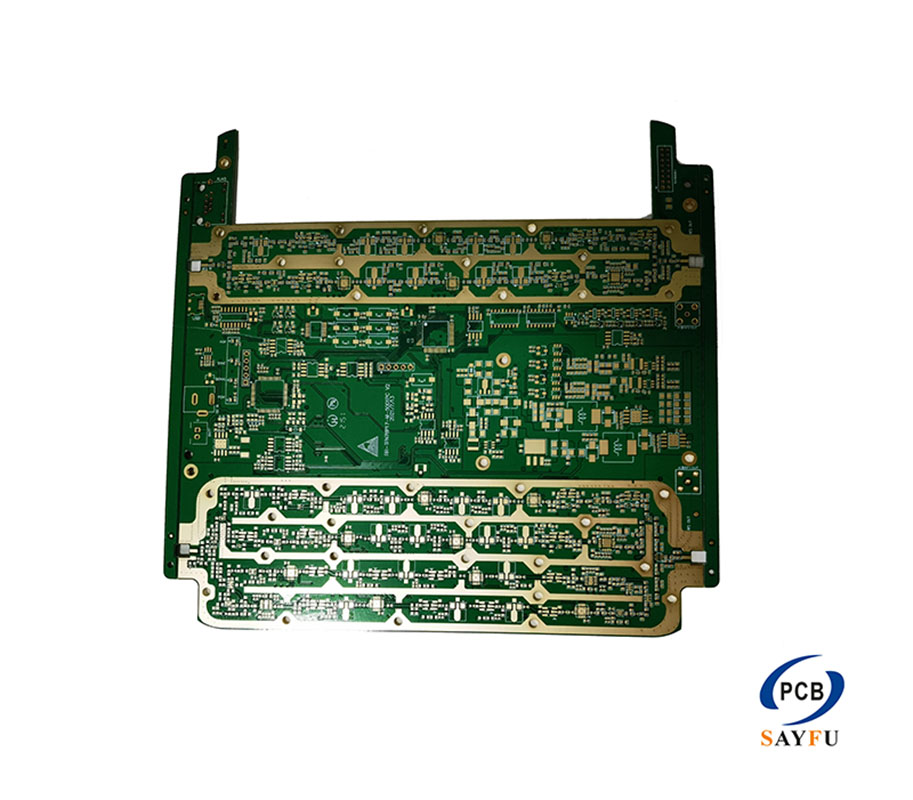
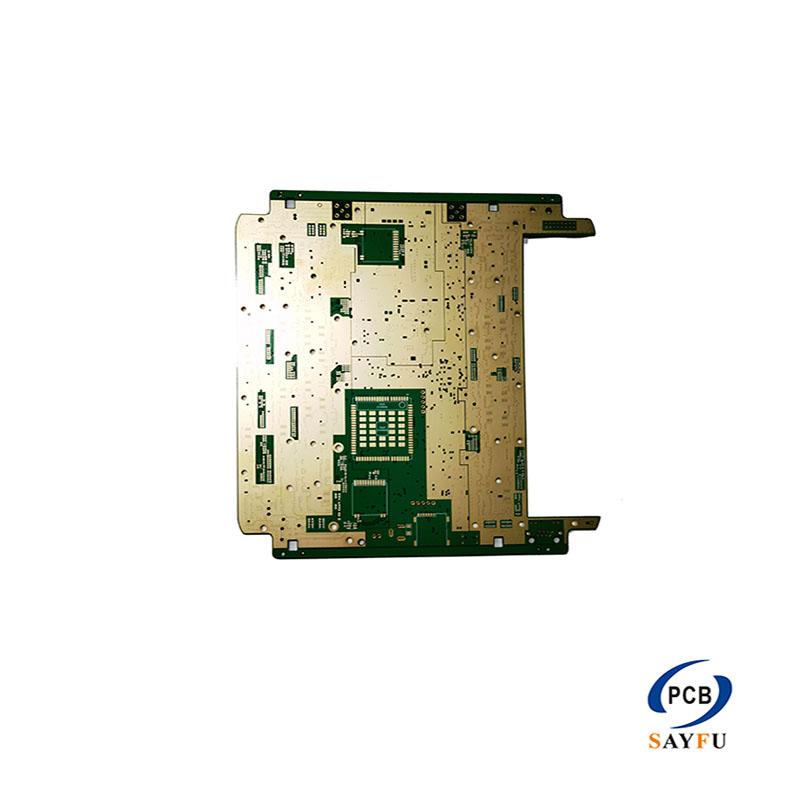
HDI circuit board Processes:
There are too many procedures of HDI circuit board fabrication. We will list the processes in a clear simple way:
Circuit Design & Engineering
Start with CAD (Computer-Aided Design) software (e.g., Altium, Cadence) to define: Circuit layout, component placement, and signal routing.
HDI circuit board-specific features: Blind vias (connecting outer to inner layers), stacked vias (overlapping holes for dense interconnection), and microvia diameters (often ≤0.1mm).
Compliance with standards (e.g., IPC-6012 for HDI quality).
Core Manufacturing Steps
The process focuses on achieving high density and reliability, with key sub-steps:
Lamination: Bond multiple layers of substrate (e.g., FR-4) and thin copper foil (12-35μm) under controlled heat/pressure to form a multi-layer base.
Pattern Transfer: Use photolithography to transfer circuit designs from CAD files to the board:
Apply a light-sensitive resist (photoresist) to the copper layer.
Expose the resist to UV light through a photomask (with the circuit pattern).
Develop the resist to leave a protective layer on the copper traces.
Etching: Remove excess copper (not covered by resist) using chemical solutions (e.g., ferric chloride), leaving precise conductive traces.
Microvia Drilling: Create blind/stacked vias using laser drilling (for <0.1mm holes) or mechanical drills (for larger holes). Laser drilling ensures high precision for dense HDI layouts.
Plating:
Electroless Copper Plating: Deposit a thin, uniform copper layer on via walls to enable conductivity (critical for blind/stacked vias).
Electrolytic Copper Plating:增厚 (thicken) the copper layer on traces and vias to meet current-carrying requirements.
Surface Finish: Apply finishes like ENIG (Electroless Nickel Immersion Gold) or OSP (Organic Solderability Preservative) to protect copper and ensure solderability.
Component Assembly
Mount electronic components (e.g., ICs, resistors) onto the HDI board using:
SMT (Surface Mount Technology): The dominant method for HDI circuit board, where components are soldered to the board’s surface via reflow ovens.
THT (Through-Hole Technology): Used for larger components (e.g., connectors) that require stronger mechanical support.
Testing & Quality Control
Rigorous testing ensures the HDI PCB meets performance and reliability standards:
Flying Probe Testing: Use automated probes to check for short circuits, open circuits, and continuity.
Electrical Testing: Verify signal integrity (e.g., impedance matching) and power delivery (e.g., voltage drop).
Functional Testing: Simulate real-world operation to ensure the board works with connected components (e.g., GPUs, CPUs).
Final Inspection & Packaging
Visual inspection (automated or manual) to check for defects (e.g., solder bridges, misaligned components).
Packaging in anti-static materials to protect the board during shipping.
This (process) emphasizes precision, especially in microvia drilling and lamination, to meet the demands of high-density applications like AI servers, smartphones, and automotive electronics. The use of advanced technologies (e.g., laser drilling, photolithography) and strict quality control ensures HDI PCBs deliver the performance required for modern electronic devices.
If you want know more information, pls contact:yana