Flexible PCB Board (Flex PCBs) have become indispensable in modern electronics, enabling the sleek designs of smartphones, foldable devices, and wearable technology. Unlike their rigid counterparts, these circuits can bend and flex, thanks to a unique manufacturing process centered on a flexible base material. The creation of a Flex PCB is a precise, multi-stage operation that ensures reliability and performance in dynamic applications.
1.Material Selection and Preparation for Flexible PCB Board
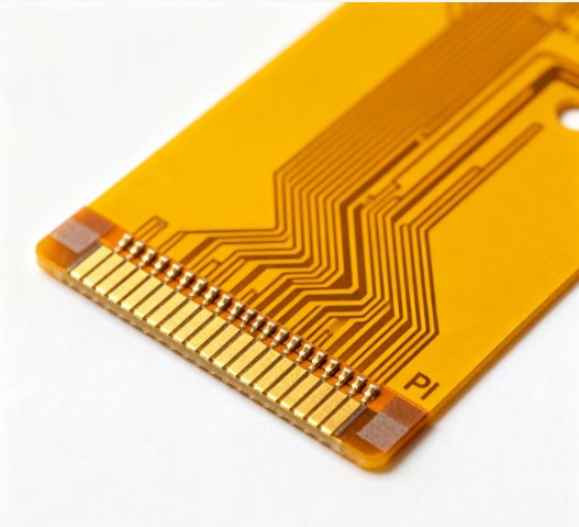
The journey begins with the core material: the flexible substrate. Instead of the rigid FR-4, Flex PCBs use a thin, flexible polymer film, most commonly Polyimide (PI). Polyimide is chosen for its excellent thermal stability, electrical insulation, and resistance to cracking when repeatedly bent. A thin layer of copper is laminated to one or both sides of this film using a heat-activated adhesive or, in higher-performance boards, a direct deposition process without adhesive (adhesiveless lamination). This copper-clad laminate forms the blank canvas for the circuit.
2.Patterning the Circuit for Flexible PCB Board
The next step is to transfer the circuit design onto the copper layer. This is achieved through a process nearly identical to rigid PCB fabrication: photolithography. A light-sensitive photoresist is applied to the copper. The circuit pattern is then exposed onto the board using UV light through a photographic film. The unexposed photoresist is then developed away, leaving a protective mask of the desired circuit pattern. The board is then placed in an etching solution, which removes the unwanted, unmasked copper, leaving only the intricate copper traces behind.
3.Adding Layers and Protection
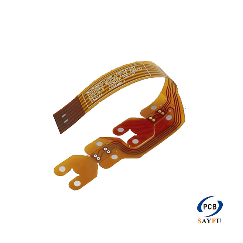
For multilayer flex designs, the separate, patterned layers are meticulously aligned and laminated together under high pressure and temperature. Following this, the critical protective layer is applied: the coverlay. Analogous to the solder mask on a rigid PCB, the coverlay is a flexible, typically polyimide, layer coated with an adhesive. It is laminated over the circuit traces to insulate and protect them from environmental factors like moisture and abrasion. Openings are punched or drilled in the coverlay to expose pads for component soldering.
4.Final Fabrication and Testing
The final stages involve creating the board outline, or profile, which is often done using a precision CNC laser cutter or a specialized die. This step cuts the individual flexible circuits from the larger panel. Holes for vias (electrical connections between layers) and component mounting are also drilled or lasered at this stage. Finally, each board undergoes rigorous electrical testing to check for short or open circuits, ensuring the flexible product meets all specified performance criteria before it is shipped for component assembly.