Essential rules and considerations for Multilayer PCB design is what the designer need to grasp when they are determine to design a correct draft and change it to Gerber files for production. The design of a multilayer Printed Circuit Board (PCB) is a critical determinant of its performance, reliability, and manufacturability. Adhering to fundamental rules is paramount for success.
The Begaining Of Multilayer PCB Design
The process begins with a meticulously planned “stack-up”. A symmetrical arrangement of core and prepreg layers around the center is crucial to prevent board warpage. Every signal layer should be adjacent to a solid reference plane, typically ground. This provides a controlled impedance and a clear return path for high-speed signals, minimizing electromagnetic interference (EMI) and crosstalk.
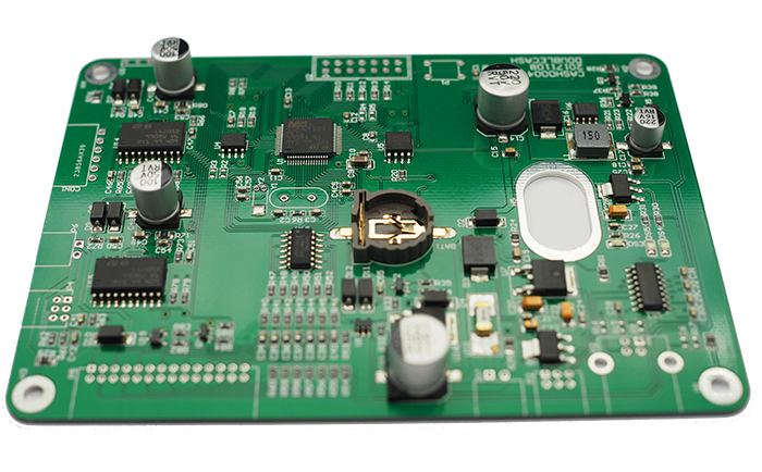
During The Component Placement
During “Component Placement”, group related circuits functionally. Position critical components like processors and memory chips first, ensuring short and direct paths for high-speed traces. Interfaces and connectors should be placed near the board edge. This logical placement simplifies the subsequent routing process.
The Routing Discipline
“Routing” requires strict discipline. For high-speed signals like clocks and differential pairs, adhere to impedance control rules by calculating trace width based on your stack-up. Maintain this impedance consistency by avoiding unnecessary vias and layer changes. Follow the “3W Rule” (spacing traces three times the width) to reduce crosstalk. Always route over continuous reference planes; never cross splits in the power or ground plane.
Power integrity is maintained by placing “decoupling capacitors” as close as possible to IC power pins, with their grounds connected directly to the plane via short, low-inductance paths. Use multiple vias for power connections to reduce impedance and improve current handling.
DRC Rules Of Multilayer PCB Design
Finally, a comprehensive “Design Rule Check (DRC)” is non-negotiable. This validates clearances, widths, and other manufacturing constraints. Furthermore, always consult your PCB fabricator early to align your design with their “Design for Manufacturability (DFM)” guidelines, ensuring a smooth transition from design to a physical, reliable board.
By systematically applying these rules—from stack-up planning to disciplined routing and rigorous checking—designers can create robust, high-performance multilayer PCBs that meet the demands of modern electronics.