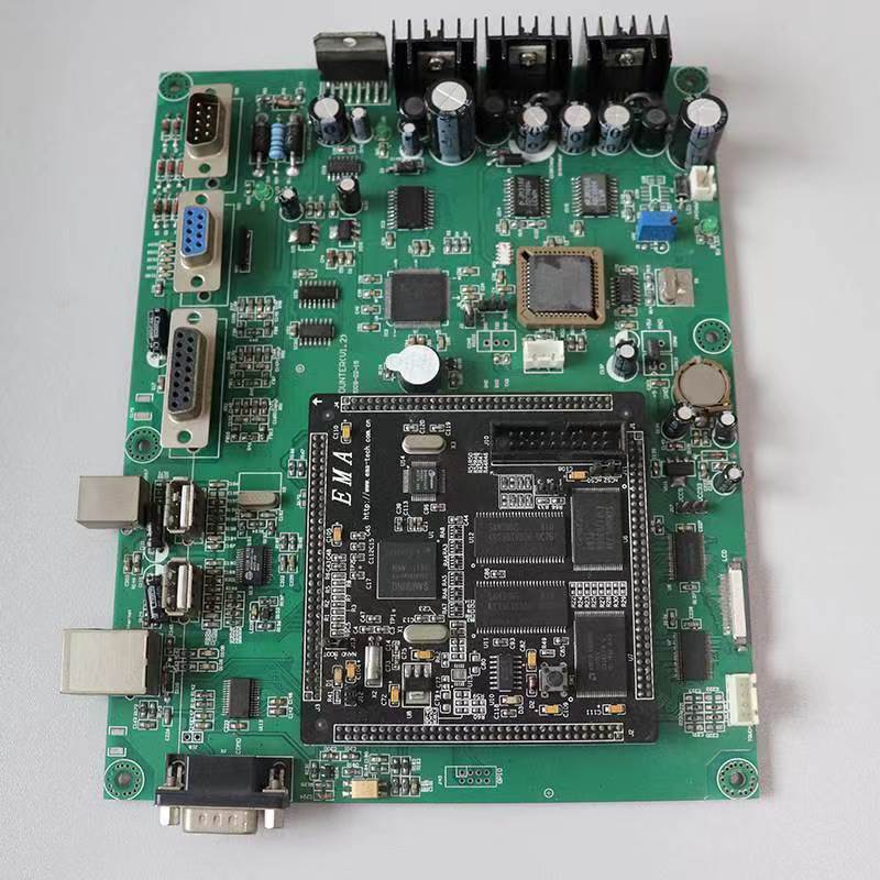
Try to Design Layer Stack-up is a critical step in ensuring signal integrity, power integrity, and EMC performance in modern electronic circuits. A well-planned stack-up provides stable return paths, minimizes crosstalk, and reduces electromagnetic emissions.
A typical multilayer stack-up includes signal, power, and ground layers arranged symmetrically to prevent board warping. For instance, a standard 4-layer board often places signals on the outer layers, with solid ground and power planes internally. This offers good shielding and controlled impedance for high-speed signals. For more complex designs, such as 6 or 8-layer boards, additional ground planes can be inserted between signal layers to further reduce noise and improve signal quality.
Try to Design Layer Stack-up, the key considerations include the dielectric material, layer thickness, and trace width. Which collectively determine characteristic impedance. Using prepreg and core materials with consistent dielectric constants helps maintain impedance matching across layers. Proper decoupling capacitor placement near power pins is also essential for minimizing power supply noise.
Basic information about PCB stackups:
PCB is build from three basic materials: Copper foil, Prepreg, Core Standard Copper foil thickness: 5um, 12um, 18um, 35um, 70um. Standard prepreg thickness: 65um, 100um, 180um. Standard core thickness: 0.15mm, 0.20mm, 0.36mm, 0.46mm, 0.56mm, 0.71mm, 1mm, 1.2mm, 1.5mm, 2.0mm, 2.4mm, 3.2mm. Core is supplied with copper foil on both sides. For some cores you need to add copper foil thickness (18um or 35um) to the core thickness.
PCB stackup examples.
Standard 4 Layer PCB stackup [mm] Standard 6 Layer PCB stackup [mm] Standard 8 Layer PCB stackup [mm].
Copper foil
0.18 prepreg
0.18 prepreg
0.71 core
0.18 prepreg
0.18 prepreg
Copper foil Copper foil
0.10 prepreg
0.10 prepreg
0.36 core
0.10 prepreg
0.10 prepreg
0.10 prepreg
0.36 core
0.10 prepreg
0.10 prepreg
Copper foil Copper foil
0.10 prepreg
0.10 prepreg
0.20 core
0.10 prepreg
0.10 prepreg
0.20 core
0.10 prepreg
0.10 prepreg
0.20 core
0.10 prepreg
0.10 prepreg
Copper foil
Ultimately, a thoughtfully designed stack-up not only enhances performance but also simplifies compliance with EMC standards, reducing the need for extensive post-design corrections.
