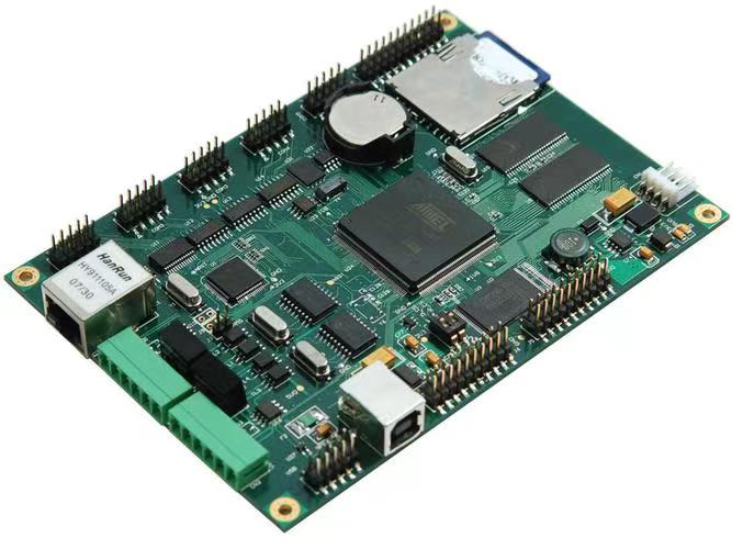
Design and application of High Frequency PCB are 2 quite important but total different fields. High Frequency PCB are specialized circuit boards designed to reliably transmit signals in the high frequency (HF) range, typically defined as frequencies above 1 GHz. Their design and fabrication represent a significant departure from standard PCBs, driven by the unique challenges posed by high-speed digital and analog RF/microwave applications.
The core principle in High Frequency PCB design is controlling signal integrity. At elevated frequencies, signals are no longer simple electrical flows; they behave as electromagnetic waves. This makes the PCB substrate itself a critical component. Standard FR-4 material, with its relatively high and inconsistent Dielectric Constant (Dk) and significant Dissipation Factor (Df), causes substantial signal loss, distortion, and phase instability. Therefore, high frequency laminates like Rogers, Teflon (PTFE), or ceramic-filled hydrocarbons are essential. These materials offer a stable Dk, low Df, and minimal moisture absorption, ensuring minimal signal degradation.
Impedance control is another cornerstone. To prevent signal reflections, we must match the characteristic impedance of transmission lines (like microstrips or striplines) must be precisely to the source and load. This requires meticulous calculation and control of the trace width, copper thickness, and the dielectric thickness of the substrate. Any variation acts as an impedance discontinuity, degrading the signal.
Furthermore, skin effect and surface roughness become significant. At high frequencies, current flows predominantly on the surface of a conductor (skin effect). Using smooth, low-profile copper foil minimizes losses associated with this phenomenon. Proper grounding, the use of ground planes, and strategic via placement are also crucial for managing return paths and minimizing electromagnetic interference (EMI).
The applications of High Frequency PCBs are vast and growing. They are the backbone of modern wireless communication systems, including 5G infrastructure, satellite communication, and radar systems. In computing, they are indispensable for high-speed servers, network routers, and data centers handling gigabits of data. Consumer electronics like smartphones and Wi-Fi routers also rely on them for their RF front-end modules.
In conclusion, High Frequency PCB design is a sophisticated discipline focused on material science and electromagnetic theory. By carefully selecting substrates and meticulously controlling geometry and impedance, engineers can create the reliable, high-speed interconnects that power our connected world.
