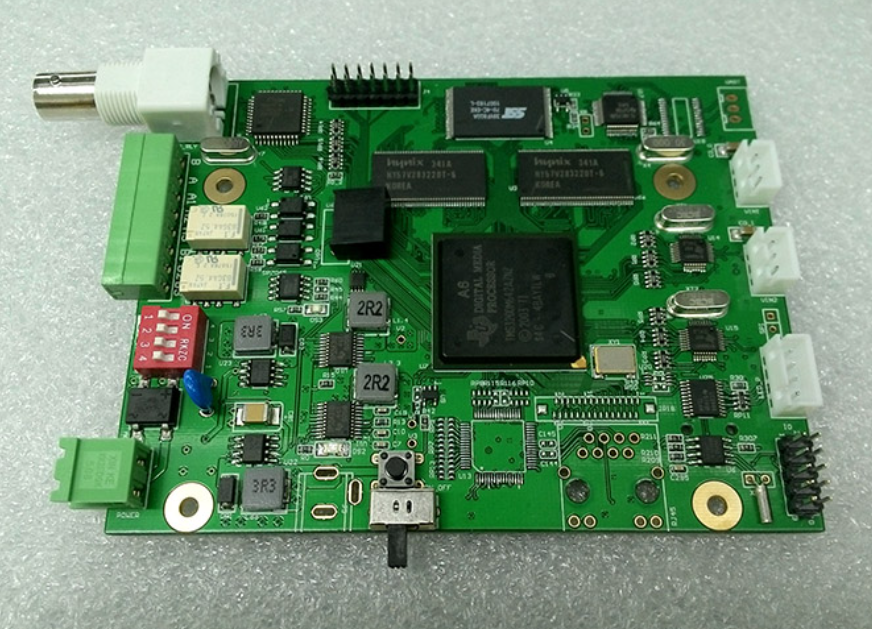
Causes and solutions for PCB film deformation In the printed circuit board (PCB) manufacturing process, phototooling films (also known as artwork films or simply “films”) are critical for transferring the circuit pattern onto the copper-clad laminate. Any deformation in these films directly leads to misregistration, resulting in defects like short circuits, open circuits, or poor alignment between layers. Understanding the causes of film deformation and implementing effective countermeasures is essential for maintaining high production yields.
1. The Causes For PCB Film Deformation
The primary cause of film deformation is variations in temperature and humidity. Phototooling films, typically made from polyester substrates like PET, are highly sensitive to environmental conditions. They expand with increasing temperature and humidity and contract when these factors decrease. If the environment where the films are stored or used differs from the environment of the PCB laminate or the exposure machine, the film and the board will expand or contract at different rates, causing misalignment. For instance, a film brought from a cool, dry storage room into a warm, humid production area will quickly absorb moisture and expand.
Other significant factors include improper handling and storage. Physically stretching the film during handling, rolling it too tightly, or storing it horizontally under weight can cause permanent mechanical distortion. Furthermore, the aging of the film material itself can lead to dimensional instability over time.
2. The Solutions For PCB Film Deformation
To combat these issues, we will require a multi-faceted approach. The most crucial solution is strict environmental control. The entire process from film plotting, storage, and handling to the exposure room. Should be maintained at a standardized, stable temperature and relative humidity (RH). A common standard is 20°C ±2°C and 50% RH ±5%. All materials, including the raw PCB laminates, should be acclimatized in this controlled environment for at least 24 hours before processing to ensure they are in dimensional equilibrium.
Improving handling procedures is equally important. Films should always be handled by their edges to avoid stress on the imaging area. They should be stored vertically in dedicated cabinets or racks, preventing any physical pressure that could cause distortion. Furthermore, implementing a first-in-first-out (FIFO) inventory system ensures that older films are used before they can degrade.
For advanced multi-layer boards, compensation techniques are often employed. By analyzing the direction and magnitude of the deformation trend. The CAM (Computer-Aided Manufacturing) data can be scaled or adjusted inversely before plotting a new film. This pre-emptive correction can effectively neutralize the predictable deformation.
In conclusion, PCB film deformation is predominantly an environmental and procedural challenge. By establishing a stable production climate, enforcing careful handling protocols, and utilizing modern compensation software. Manufacturers can significantly reduce registration errors, thereby enhancing product quality and production efficiency.
