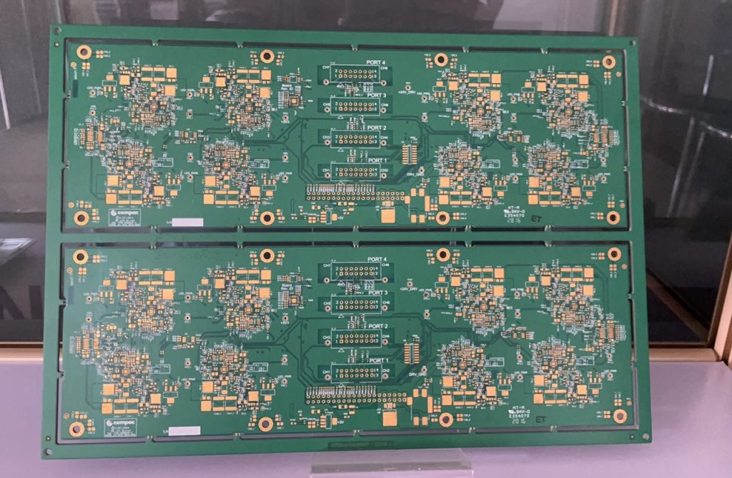
Blind Vias PCB manufacturer, At the heart of high-end electronic devices, multilayer PCBs carry signals and energy through dense circuits. Traditional through-holes penetrate the entire board, limiting wiring space. To achieve higher density and performance, advanced interconnection technologies such as buried vias and blind vias have emerged, becoming key to modern high-density circuit design.
Hidden Bridges: Buried Vias
Blind vias connect the outermost layer of a PCB to one or more inner layers but do not penetrate the entire board. They are visible from the surface but not on the bottom. Buried vias, on the other hand, are entirely hidden within the PCB, connecting only different inner layers and completely undetectable from the board’s surface. These technologies are like adding express elevators and inter-floor stairways in a skyscraper, avoiding the need to pass through every floor when moving from the top to the bottom.
Why Are Complex Vias Needed for Blind Vias PCB manufacturer
The primary reason for using these complex vias is to free up valuable wiring space. They avoid occupying significant areas on all layers, providing more channels for routing. Secondly, they significantly improve signal integrity. By shortening the transmission paths of critical signals (such as high-frequency clocks), signal reflection and attenuation are reduced. Additionally, they help lower the overall board thickness, meeting the demands of slim and lightweight devices.
The Engine Driving High-Density Design for Blind Vias PCB manufacturer
The maturation and application of buried and blind via technologies have enabled devices like smartphones and ultra-thin laptops to become increasingly powerful while continuing to shrink in size. As the core of modern high-density interconnection, they directly elevate the level of PCB design and manufacturing, serving as a critical foundation for the ongoing innovation of future electronic products.
These advanced via technologies, combined with HDI processes, enable unprecedented miniaturization of electronic devices while maintaining superior performance. As we move toward the era of 5G and IoT, they will continue to play a pivotal role in creating more compact, powerful, and reliable electronic products that connect our world in smarter ways.