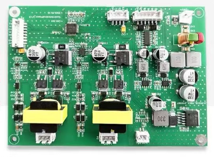
Assembly of PCB is the specialized process of populating and soldering electronic components onto a bare board.. This journey from an inert substrate to a dynamic, interconnected component involves a series of precise, automated, and meticulously controlled steps. Understanding this process is key to appreciating the complexity behind modern technology.
Stage 1: The Foundation of Assembly of PCB
The first decisive step in the assembly of a PCB is the application of solder paste. This is not simple glue; it is a carefully formulated mixture of tiny solder spheres and flux. The process uses a stencil, a thin metal sheet with laser-cut holes that align precisely with the component pads on the board. A squeegee moves across the stencil, pushing the paste through these holes and onto the board. The accuracy of this stage is paramount, as too much paste can cause shorts, and too little can result in weak connections. This initial step lays the literal and metaphorical foundation for all subsequent components, making it a critical phase in the precise assembly of PCB.
Stage 2: Automated Component Placement
Once the solder paste is deposited, the board moves to the pick-and-place machine. This is where automation and speed truly shine. These robotic systems use pre-programmed instructions to pick surface-mount devices (SMDs) such as resistors, capacitors, and integrated circuits from reels or trays and place them onto their designated locations on the solder paste at incredible speeds. Modern machines can place tens of thousands of components per hour with sub-millimeter accuracy. This high-speed, high-precision placement is essential for the efficiency and reliability of the mass assembly of PCB, ensuring that every microchip and minuscule resistor is positioned correctly before the permanent bonding occurs.
Stage 3: The Reflow Soldering Process
With all components in place, the board is on a conveyor belt through a reflow oven. This is not a simple heating process; it is a carefully controlled thermal profile. The board passes through several zones:
- Preheat: Gradually raises the temperature to activate the flux.
- Thermal Soak: Evaporates solvents and equalizes the temperature across the board.
- Reflow: The temperature peaks (typically 240-250°C), melting the solder particles in the paste and forming a permanent metallurgical bond between the component leads and the PCB pads.
- Cooling: A controlled cooldown solidifies the solder joints, creating strong and reliable electrical connections.
This transformative process turns the paste into solid solder joints, permanently fixing the components to the board.
Stage 4: Inspection, Testing, and Final Assembly of PCB
After reflow, the quality of the assembly of the PCB must be verified. Automated Optical Inspection (AOI) systems use high-resolution cameras to check for common defects like misaligned components, bridging, or insufficient solder. For more complex boards with hidden connections, X-ray inspection might be used to examine solder joints under Ball Grid Array (BGA) packages.
Through-hole components are installed and soldered, often manually or with specialized machines.. Finally, functional testing is performed. Power is applied, and the board is tested against its design specifications to ensure it operates as intended. This rigorous validation is the final, crucial step that guarantees the quality and functionality of the completed assembly.
Conclusion: More Than Just Assembly
The modern assembly of PCBs is a sophisticated symphony of engineering, robotics, and materials science. This automated process creates the reliable electronics we use.. From smartphones to life-saving medical devices, the precision and care embedded in each step of PCB assembly are what bring our digital world to life.