2 layers rigid PCB with white solder masking
Images
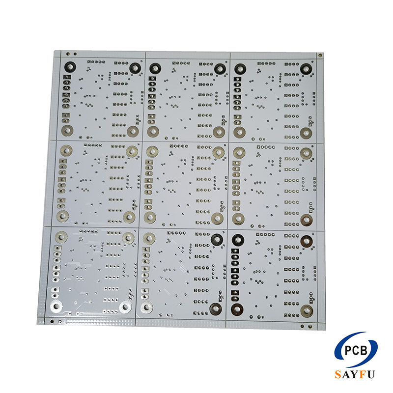
General Specification:
- Layers:2L
- Material : FR4
- Finished Thickess :1.6MM
- Finished Copper :1oz
- Surface treatment : ENIG
- Soldermask : White soldermask
One-Stop&High-End PCB Manufacturer SAYFU Advantage:
SAYFU is a PCB manufacturer located in Shenzhen since 2001.With ISO 9001:2015, AS9100, TS16949 and ISO13485, we can support different customer requirement. We can cover all kinds of high- tech technologies: Rigid multi-layer PCB, Flex PCB, Hybrid PCB, HDI board,Heavy Copper PCB etc.
Payment term:TT 30-60 days payment term after shipment(No deposit )
Around 500 full time staff with a capacity of 60ksqm per month, 12,000 square meter of factory
SAYFU is a professional PCB supplier from 1 layer up to 24 layer including special HDI technology, special material like rogers, ISOLA, M4, M6.
Key information for you about SAYFU:Total 20 years’ experience on multi-layer PCB industry.
With 20 years experience on PCB business.
Very flexible on all kinds of order volumes with very aggressive cost.
Support both FOB HK and DAP service
A professional quality team to guarantee reliable quality.
- Layer counts: 1-38 Layers
- Maximum size: 550x1600mm
- Material: CEM1,CEM3,FR-4,High Tg FR-4,Halogen free,High Frequency(Rogers,Arlon,Taconic,Nelco…), Aluminium base, Copper base
- Board outline tolerance: ±0.10mm
- Board thickness: 0.1-6.0mm
- Thickness tolerance: ( t ≥0.8mm) ±8%
- Thickness tolerance: ( t <0.8mm) ±10%
- Out layer copper thickness : H oz -20 oz
- Inner layer copper thickness: 1/2 oz -10oz
- Minimum line/ space: 0.075mm
- Minimum finished hole: (mechanical) 0.15mm
- Minimum finished hole: (laser) 0.1mm
- Aspect ratio:15:1
- Impedance control tolerance: ±10%
- Bow and twist: Max. 0.7%
- HDI PCB stack up: 1+N+1,2+N+2,1+1+N+1+1,3+N+3
- Surface Treatment: HASL,HASL Lead Free, ENIG,Immersion Silver,Immersion Tin,Flash Gold,Golden Finger,OSP,Carbon Ink, Peelable Mask.
- Microvia & ELIC technology
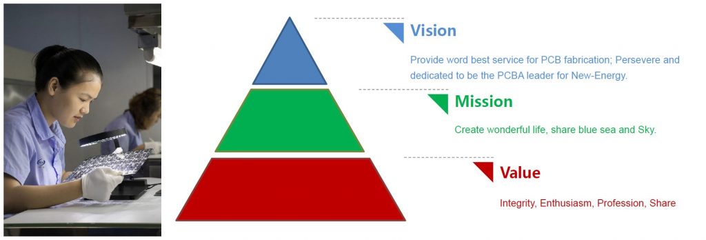
PCB Prototype Manufacturer Sayfu multilayer PCB Enterprise culture
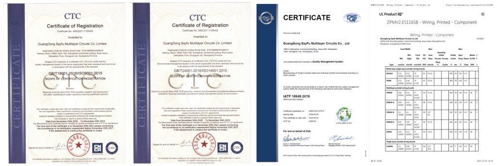
SAYFU 2 layers rigid PCB – Certification of high quality PCB international quality systems
The certification of international quality systems including UL E511658, ISO9001, ISO14001, IATF16949:2016
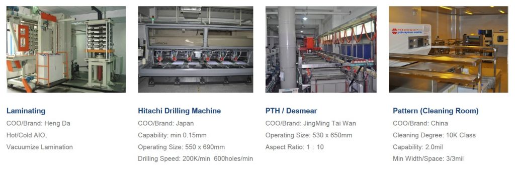
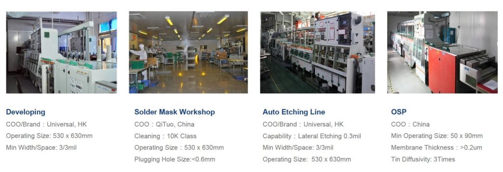
Part of 2 layers rigid PCB industry’s production line
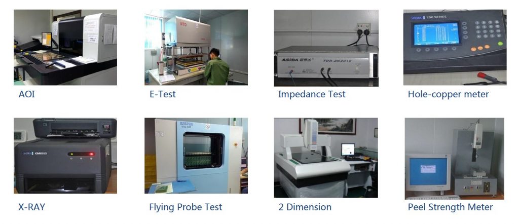
Part of a circuit board factory test machines
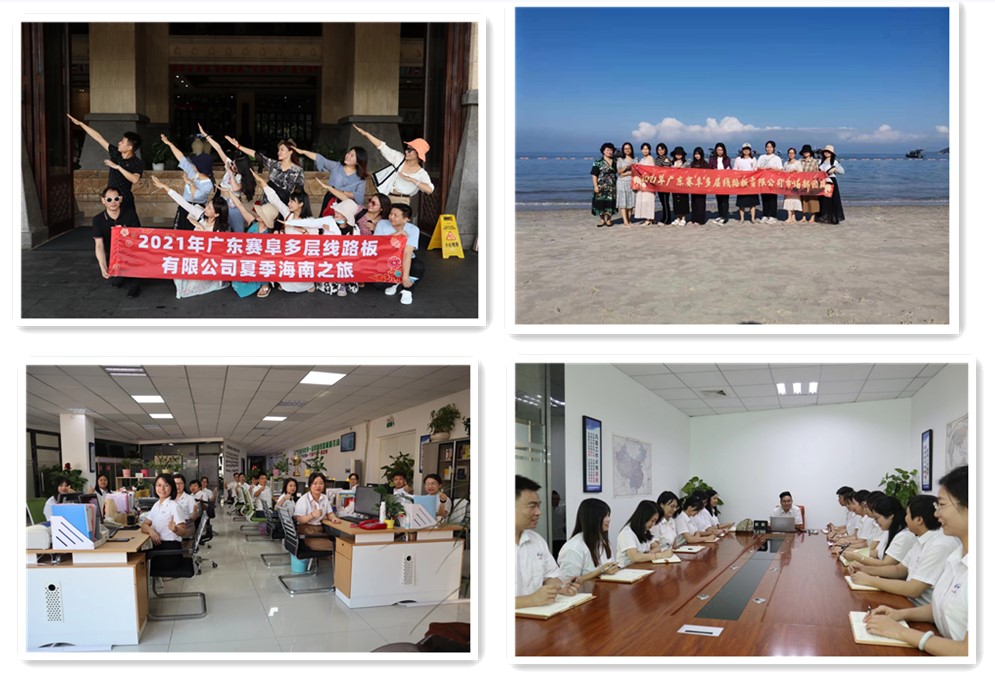
China top class multilayers PCB manufacturer International Sales Team