Today, China’s packaging and testing industry faces policy opportunities, market opportunities and technological opportunities. In terms of policy opportunities, from 2016 to 2020, relevant departments are releasing new integrated circuit industry policies, which have provided strong support for the packaging and testing industry, and new policies are still being introduced.
In terms of market opportunities, China’s packaging industry has a lot of room for development. It is understood that China’s integrated circuit imports in 2021 will be 635.48 billion pieces, a year-on-year increase of 16.9%, and the GAGR from 2013 to 2021 will be 11.3%. In 2021, China’s integrated circuit imports will amount to US$432.55 billion, a year-on-year increase of 23.6%, and the GAGR from 2013 to 2021 will be 9.4%. High-end integrated circuit products required by the domestic market, such as general-purpose processors, memory and other key core products, still rely on imports. Therefore, the localization development potential of China’s packaging industry is huge.
In terms of technological opportunities, since the development of Moore’s Law has encountered bottlenecks, the chip feature size has approached the physical limit, and advanced packaging technology has become an important way to continue Moore’s Law. This also brings good opportunities for packaging and testing companies, and advanced packaging and testing technology has become a hot spot in the industry. In the next 10 to 20 years, the development of heterogeneous integration technology will be significantly accelerated.
Under the combined effect of these three major opportunities, China’s packaging and testing industry has also ushered in a new accelerated development.
The proportion of design, manufacturing, packaging and testing industries is becoming more and more reasonable
Previously, China’s semiconductor industry paid more attention to the chip design industry than the chip manufacturing and chip packaging and testing industries, and this phenomenon is gradually improving.
Today, the proportion of the three industries (design/manufacturing/packaging and testing) in China’s integrated circuit industry is more reasonable. Statistics from the China Semiconductor Industry Association show that the sales of China’s integrated circuit industry in 2021 will be 1,045.83 billion yuan. Among them, the design industry, manufacturing industry, packaging and testing industry accounted for 43.2%: 30.4%: 26.4%.
The reasonable proportion of the three industries in the world’s integrated circuit industry (design: wafer: packaging and testing) is 3:4:3. It can be seen that the proportion of China’s integrated circuit packaging and testing industry is still in an ideal position in the IC manufacturing industry.
Today, the distribution area of the domestic packaging and testing industry is mainly concentrated in the Yangtze River Delta region. The total sales of the packaging and testing industry in Jiangsu, Shanghai and Zhejiang in 2020 will reach 183.83 billion yuan, accounting for 73.3% of the sales of my country’s packaging and testing industry in 2020.
According to statistics from the Jiangsu Semiconductor Industry Association, as of the end of 2020, there were 492 semiconductor packaging and testing companies in China, of which 71 new companies entered semiconductor packaging and testing (including production/under construction/signing contracts) in 2020. When the number of packaging and testing enterprises in Jiangsu was the largest, there were 128, followed by 97 in Guangdong, 48 in Shandong, 40 in Anhui, 38 in Shanghai and 34 in Zhejiang. As of now, the data for 2021 has not been released, but the overall distribution of the national packaging and testing industry remains unchanged.
TSMC: The first batch of advanced packaging to enter the market(China’s integrated circuit packaging)
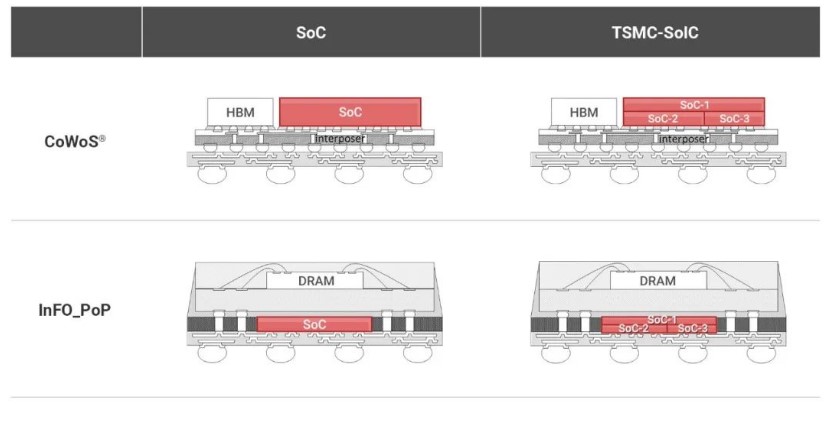
As a leader in wafer manufacturing, TSMC is also one of the first upstream manufacturers to start deploying advanced packaging. At present, CoWoS has developed to the fifth generation, and TSMC has integrated its own advanced packaging technology into a 3DFabric technology platform, including TSMC’s front-end SoIC technology and back-end CoWoS and InFO packaging technologies.
It is reported that the earliest introduced CoWoS is a packaging technology based on TSV (through silicon via), which is mainly used for high-performance computing because it can flexibly adapt to multiple types of chips such as SoC, chiplets, and 3D stacks. (HPC) and artificial intelligence (AI) computing fields.
CoWoS is the most widely used 2.5D packaging technology today, and products from NVIDIA, Broadcom, Google, Amazon, NEC, AMD, Xilinx, Habana and other companies have adopted this technology. Most of the high-performance chips using HBM, including the AI training chips of most startups, use CoWoS technology.
Relatively speaking, CoWoS has better performance but higher cost; InFO uses RDL (redistribution layer) instead of silicon interposer without TSV, which is more cost-effective. The technology also helped TSMC grab orders from Apple, now its largest customer.
Compared with CoWoS and InFO technologies, SoIC can provide higher packing density and smaller bond spacing. SoIC is the key to TSMC’s heterogeneous chiplet packaging with high-density vertical stacking performance. This technology helps the chip achieve high performance, low power consumption and minimal RLC (resistance, inductance and capacitance).
More importantly, SoIC and CoWoS/InFO can be shared, and the SoIC-based CoWoS or InFO package will bring a smaller chip size and realize the integration of multiple small chips.
Samsung: Advanced packaging has four options
After failing to compete for Apple’s A-series processor orders, Samsung Electronics established a special working group in 2015 to develop the first-generation panel-level fan-out package (FOPLP) with Samsung Electro-Mechanics as the main force.
The technology was first used in the Galaxy Watch smartwatch. Through FOPLP technology, Samsung integrates the Galaxy Watch’s power management circuit (PMIC), application processor and dynamic random access memory (DRAM) into the same large package.
Specifically, Samsung’s advanced packaging includes four solutions: I-Cube, X-Cube, R-Cube and H-Cube.
For its own advanced packaging products, Samsung Electronics offers two business models. First, customers can choose packaging products from the foundry department of Samsung Electronics or products from packaging and testing partners such as Amkor; second, customers can hand over COT (customer-owned tools), COPD (customer-owned physical tools) design) model acquisition.
According to Korean media reports, Samsung Electronics has established a new test and packaging (TP) center in the DS (Semiconductor Business and Device Solutions) business unit, intending to compete with TSMC in the field of advanced packaging.
Intel: AWS becomes first IFS packaging customer
Shortly after the official disclosure of EMIB, Altera, the heavyweight customer of Intel’s foundry business and the FPGA leader at the time, launched the industry’s first heterogeneous system-in-package chip, integrating SoC, Stratix10 FPGA and SK Hynix’s HBM2.
This chip uses Intel’s EMIB technology to realize the interconnection between DRAM and FPGA, and initially shows the performance of Intel’s advanced packaging to the outside world. Intel’s EMIB products have been shipping and iterating continuously since 2017.
Then, in July 2019, Intel shared three new advanced packaging technologies with the industry, namely Co-EMIB, ODI and MDIO.
Today, both Intel’s EMIB and Foveros have had multiple iterations. Sapphire Rapids has become Intel’s first Xeon data center processor to ship in volume, and the bump pitch of the next-generation EMIB will also be shortened from 55μm to 45μm.
Foveros has achieved second-generation deployment in Meteor Lake with 36μm bump pitch. In addition, Intel is also developing next-generation Foveros technologies, Foveros Omni and Foveros Direct.
In addition to technology, Intel has even found packaging customers. At last year’s Intel Architecture Day, AWS announced that it would be the first customer to use Intel’s Foundry Services (IFS) packaging solutions.
Advanced packaging or manufacturing of finished chips will become one of the important disruptive technologies in the post-Moore era, especially the increasingly important position of downstream finished product manufacturing in the industrial chain, which is expected to become a new commanding height of the integrated circuit industry.
Today, chip manufacturing giants such as Intel, Samsung, and TSMC are strengthening their advanced packaging. However, it is difficult for packaging and testing manufacturers to have the advantage of front-end manufacturing, and many packaging and testing players have fallen behind the first echelon in advanced packaging. Although Samsung and other manufacturing giants still emphasize cooperation with packaging and testing players, the future trend of the packaging industry is unpredictable.
Part of the content comes from: Semiconductor Industry Observation: Heroes are competing for advanced packaging, and back-end manufacturing has ushered in an inflection point; China Electronics News: Continuing Moore’s Law, but also looking at advanced packaging; China Electronics News: Advanced packaging will become the main increase in the global packaging market; Core stuff: Rush advanced packaging! TSMC, Intel, Samsung in a hurry