What is HDI PCB (HDI blind buried via PCB)? Why is there a separate category called HDI in the PCB technology category? HDI is designed to provide a lot of interconnect in a very small space. Components are placed closely on the board, which helps reduce size, but functions like a larger board. HDI PCB is the combination of various components when using general wiring. Micro-void technology, buried and blind vias make this type of sheet possible. HDIs are the best choice for PCB designers who need higher density components, they are efficient and very popular across industries.
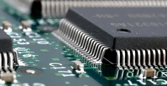
So what is the biggest advantage of HDI PCB? If you want to reduce size and weight, but still need the function and reliability of the product, then HDI PCB is a good solution. Another advantage of this circuit board is the use of pad soldering technology and blind hole technology. This keeps components together, so shortening the signal path helps deliver a faster, more reliable signal.
Despite the many advantages of such boards, you will still find them cheap. This is an economical and efficient solution, a reliable and durable choice for many electronic devices. Before choosing them though, it’s important to understand how regular editions differ from hdi boards, learn more about them and how to use them to determine if they’re a good fit.
What industries are HDI PCB used in today? A closer look reveals that HDI PCB has been used in a variety of electronic devices in many different industries. The medical industry is a very well-known industry, and the medical devices produced today are generally relatively small. Whether it’s a device, or an implant in the lab, small size is often a better choice, and HDI PCB can help a lot in this regard.
In addition to the medical industry, HDI PCB is also used in the automotive industry, aerospace and military. Their reliability and small size make them suitable for a wide variety of applications. It is believed that in the future, more and more devices in different fields will use this technology.
What is the main difference between PCB and HDI PCB? Some of the main differences between the two options are that high-density printed circuit boards have denser components per square inch, and these boards end up being smaller and lighter than typical printed circuit boards. HDI PCBs are laser drilled directly, while standard PCBs are usually drilled mechanically, so the number of layers and aspect ratios tend to be reduced.
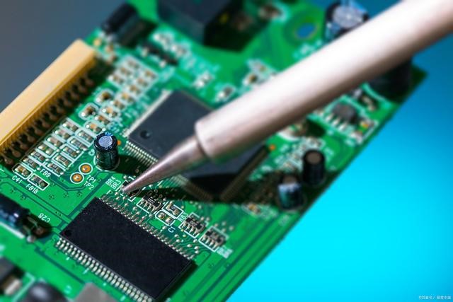
While using these types of PCBs seems like a PCB is the perfect solution, the most important thing is to know how to design it properly. If you want to achieve all the benefits, when designing this type of PCB, try to ensure that no more than three layers are used for sequential layers. Under ideal conditions, the number of consecutive laminations should be small, and the design requires time and careful thought.